
High-Temperature Coefficient of Resistance in MoxW1−xS2 Thin Film


1
Department of Electronic Engineering, National Changhua University of Education, No. 2, Shi-Da Road, Changhua 50074, Taiwan
2
Department of Electronic Engineering, National Kaohsiung Normal University, No. 62, Shenjhong Rd., Yanchao District, Kaohsiung 82444, Taiwan
*
Author to whom correspondence should be addressed.
Appl. Sci. 2022, 12(10), 5110; https://0-doi-org.brum.beds.ac.uk/10.3390/app12105110
Submission received: 22 April 2022
/
Revised: 14 May 2022
/
Accepted: 17 May 2022
/
Published: 19 May 2022
(This article belongs to the Special Issue Selected Papers from ISET 2021, TSBME 2021, ISPE 2021, SEMBA 2022, and IEDMS 2022)
Abstract
:Despite the use of transition metal dichalcogenides being widespread in various applications, the knowledge and applications of MoxW1−xS2 compounds are relatively limited. In this study, we deposited a MoW alloy on a Si substrate using a sputter system. Consequently, we successfully utilized a furnace to sulfurize the MoW alloy from 800 to 950 °C, which transferred the alloy into a MoxW1−xS2 ternary compound. The Raman spectra of the MoxW1−xS2 samples indicated an additional hybridized Raman peak at 375 cm−1 not present in typical MoS2 and WS2. With increasing sulfurization temperature, the scanning electron microscopy images revealed the surface morphology of the MoxW1−xS2 gradually becoming a sheet-like structure. The X-ray diffraction results showed that the crystal structure of the MoxW1−xS2 tended toward a preferable (002) crystal orientation. The I–V results showed that the resistance of MoxW1−xS2 increased when the samples were sulfurized at a higher temperature due to the more porous structures generated within the thin film. Furthermore, a high-temperature coefficient of resistance for the MoxW1−xS2 thin film sulfurized at 950 °C was about −1.633%/K−1. This coefficient of resistance in a MoxW1−xS2 thin film indicates its suitability for use in thermal sensors.
1. Introduction
In the past few years, transition-metal dichalcogenides (TMDCs) such as MoS2 and WS2 have been attractive subjects for experimental and theoretical studies owing to their unique electrical and optoelectronic properties [1,2]. These two representative materials of TMDCs have also been applied to aspects of next-generation ultrathin devices, including light-emitting devices [3,4], photodetectors [5], gas sensors [6], catalytics [7,8], and photovoltaic devices [9,10]. Recently, Khan et al. observed that both atomically thin MoS2 and MoTe2 layers possess a large temperature coefficient of resistance (TCR) due to the reduction in the density of Coulomb impurities and scattering centers [11]. Lee et al. drew WS2 bulk film on paper substrates, demonstrating the usability of a WS2-on-paper thermal sensor [12]. Although the above literature confirms MoS2 and WS2 are suitable for application in thermal sensors, no report related to the temperature-dependent resistance and TCR of MoxW1−xS2 compound semiconductors has been published. Compared with bulk structure, it is still challenging to fabricate thermal sensors using a few-layer structured 2D material because of the difficulty in controlling size, shape, and dimensions. In addition, the resistance variation of a material caused by heating depends on its TCR. The microstructure of a thin film and film interface strongly influence the TCR of a material [13]. Therefore, the issues related to the relationship between TCR and film morphology for both large-area and bulk MoxW1−xS2 are worth investigating.
In this work, we sulfurized a MoW alloy at different temperatures from 800 to 950 °C to transform the metallic layer into a MoxW1−xS2 compound semiconductor thin film. Raman spectrum, X-ray diffraction (XRD), and scanning electron microscopy (SEM) were implemented to observe the relevant microstructural characteristics of the samples and further understand the sulfurized mechanism. Furthermore, we utilized temperature-dependent I–V measurements to analyze the influence of the MoxW1−xS2 microstructure on resistance and TCR. A series of experimental results indicated that the large-area and bulk MoxW1−xS2 thin film has great potential as a thermal sensor.
2. Materials and Methods
We selected boron-doped single-crystal Si wafers with a native oxide layer as the substrates for further MoxW1−xS2 growth. At first, the pressure of the sputter was pumped down to 5 × 10⁻⁶ torr. Before sputtering, Ar was injected as a carrier gas and the pressure of the sputter was kept at 5 × 10⁻³ torr. Consequently, the Mo and W thin films were simultaneously deposited by using radio frequency (50 W) and direct current (25 W) sputtering methods at room temperature, respectively. The thickness of the MoW alloy film was about 100 nm.
Then, the MoW films were transferred to a two-zone vacuum furnace for further sulfurization processes to grow the MoxW1−xS2. We placed 8 g of sulfur powders at the upstream source zone while the MoW films were placed at the downstream reaction zone. We set various sulfurized temperatures of 800, 850, 900, and 950 °C for 60 min in the reaction zone for progressive sulfurization and to investigate the effect of different sulfurized temperatures on the MoxW1−xS2 films. The temperature in the source zone was set to about 400 °C. The temperature ramping rate was set to 5 °C/min for the heating and cooling procedures. Argon was injected at a fixed rate of 200 sccm as the carrier gas at a pressure of around 0.1 torr during the whole process. The sulfur vapor was transported from the source zone via the carrier gas and reacted with MoW alloy to transform into the MoxW1−xS2 thin film on the substrates in the reaction zone.
SEM (FEI Helios 1200+, Hillsboro, OR, USA) was used to observe the morphology and thickness of the as-grown samples. The Raman spectra were recorded using a confocal Raman microscopy system (Tokyo Instruments, Inc., Nanofinder 30, Tokyo, Japan) with a solid-state laser excitation (laser power: 0.05 mW). The laser beam was focused to 1 μm in diameter via a microscope objective with a magnification of 100× and an NA of 0.9. The grating in the spectrometer was 300 lines/mm. Before the Raman measurements of the samples, the spectra were calibrated using the Si peak position (520 cm−1) from a bulk Si substrate. A charge-coupled device mounted within the spectrometer was cooled to −50 °C by using a thermoelectric cooling chip to reduce noise during measurement. The relevant parameters related to sulfurization and Raman measurement can be found in our previous work [14]. The crystal structure was analyzed using XRD with CuKα radiation. Furthermore, recorded the temperature-dependent current density–voltage (I–V) characteristics of the samples from 290 to 570 K. Meanwhile, we also analyzed the electrical properties of the samples, including their resistance and temperature coefficient of resistance (TCR) according to the temperature-dependent I–V results.
3. Results and Discussion
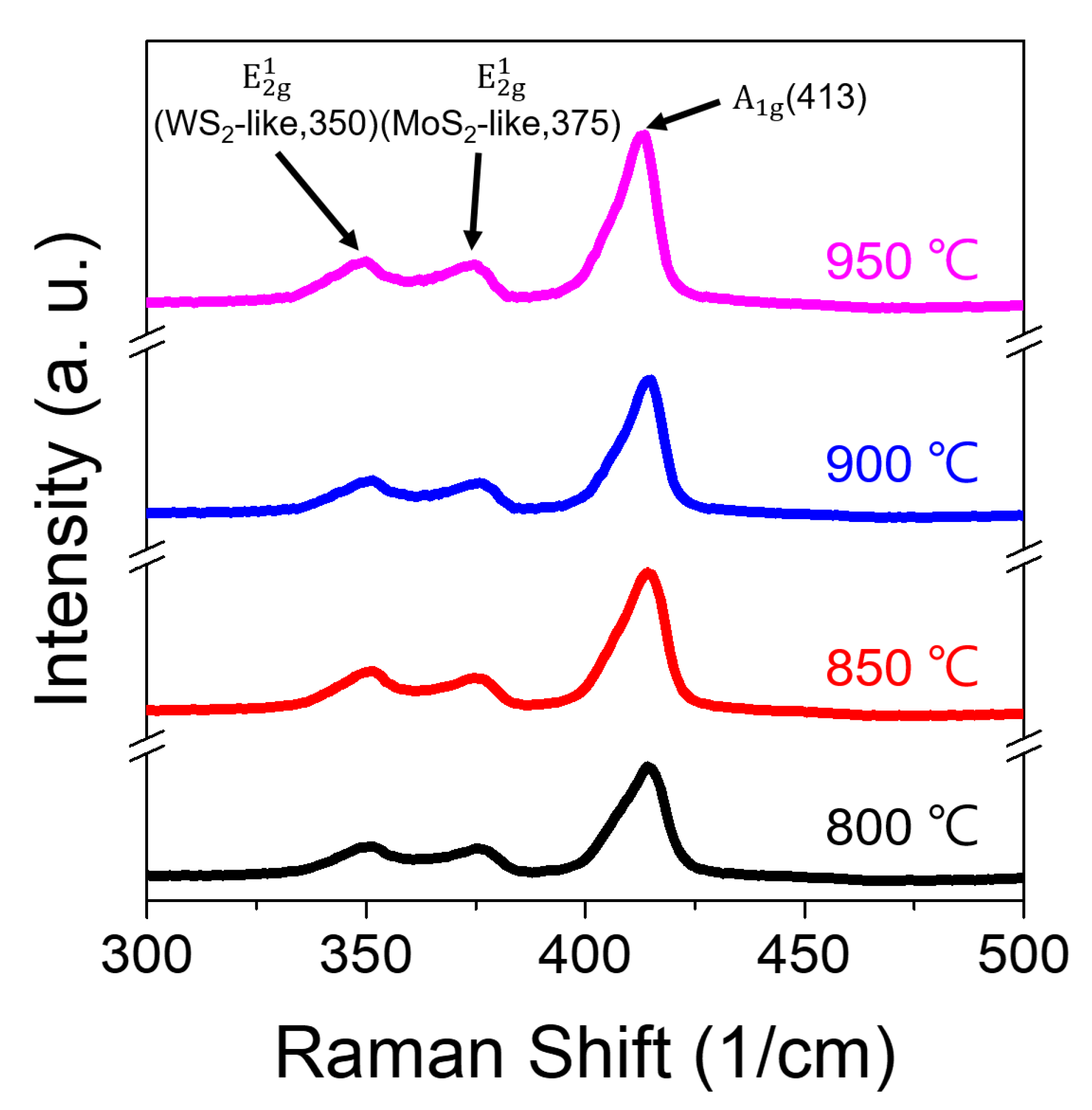
The Raman spectra of the MoxW1−xS2 thin films sulfurized at 800~950 °C are shown in Figure 1. All samples presented the same peak position with no obvious difference. The broad peak around 413 cm−1 was created by the merging of two peaks: A1g mode at 405 cm−1 for MoS2 and A1g mode of 417 cm−1 for WS2, which are associated with the out-of-plane vibration frequency. The peak around 350 cm−1 could be attributed to the in-plane vibration E12g mode of WS2. The above results are consistent with previously reported results [15,16]. However, there was a unique peak around 375 cm−1 related to MoS2, similar to that in the E12g mode. Lin et al. observed that the peak position of the MoS2-like E12g mode shifted from 383 to 373 cm−1 for the MoxW1−xS2 hybrid triangle, suggesting that the MoS2-like E12g mode could be attributed to local strain [17]. This phenomenon of mode shift was also found in uniform alloys of MoS2 and WS2 produced by chemical vapor transport [18]. Therefore, we inferred that mixing the two phases with different lattice constants resulted in the generation of the local strain when the MoxW1−xS2 thin film formed in our case, then the peak position of MoS2-like E12g was encountered at around 375 cm−1. However, the peak position of WS2-like E12g at 350 cm−1 does not shift even though the local strain exists [19]. Our Raman spectra results confirmed that our sulfurized conditions allowed the MoW alloy films to be completely sulfurized into the MoxW1−xS2 thin films because no peak correlating with the oxides of Mo or W elements could be found.
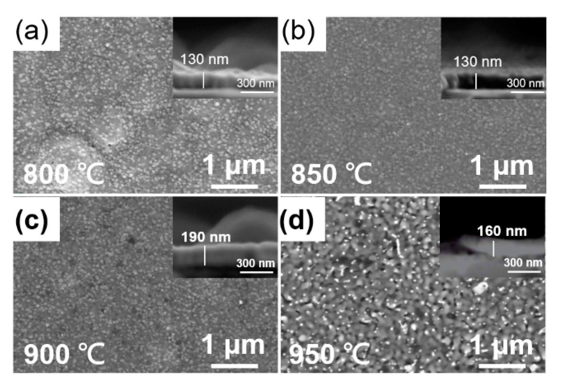
Figure 2a–d shows the SEM images of the MoxW1−xS2 thin films after various sulfurized temperatures from 800 to 950 °C. For the sample sulfurized at 800 °C, Figure 2a reveals that there were some bumps swelling on the local area. In comparison, the morphology was highly consistent for the sample sulfurized at 850 °C in Figure 2b. For sulfurized temperature above 900 °C, Figure 2c presents the porous structure formed on the sample surface, and Figure 2d reveals the crystal feature had become more clearly visible. The insert images in Figure 2a–d provide information about the thicknesses after various sulfurization temperatures. The thickness was about 130 nm when the samples were sulfurized at 800 and 850 °C. The thickness reached 190 nm when the sulfurizing temperature was 900 °C and then decreased to 160 nm after sulfurizing the MoW alloy film at 950 °C. In addition, the MoxW1−xS2 thin film was partially separated from the substrate, as shown in the insert in Figure 2d. We provide a detailed discussion about the sulfurization mechanism below.
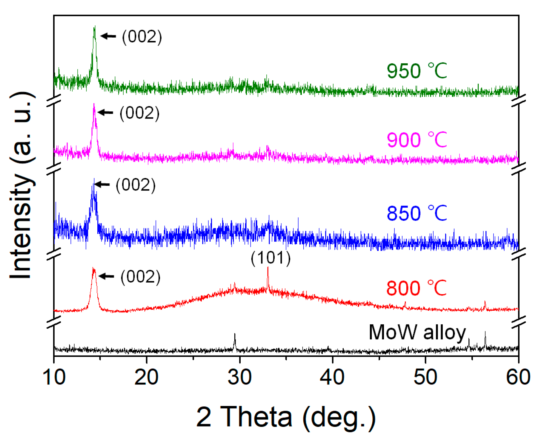
We performed XRD on our samples in ω-2θ mode to confirm the crystal orientations and determined the sulfurization mechanism for the MoxW1−xS2 thin films under various sulfurized temperatures (see Figure 3). We thought that the present (002) peak was created by merging both MoS2 and WS2 (002) phases (JCPDS No. 24-0513 and JCPDS No. 08-0237, respectively). However, it was difficult to distinguish the X value of Mo composition for the MoxW1−xS2 thin film because the spacing along (002) for both MoS2 and WS2 were very close. The samples sulfurized below 850 °C exhibited a broad peak ranging from 20° to 40°, which could be attributed to amorphous MoS2 and poorly crystallized WS2 [20,21,22]. This broad peak gradually disappeared when the sulfurized temperature was above 900 °C. As a result, the crystalline quality of MoxW1−xS2 thin film could be improved by means of adjustment to the sulfurized temperature, which is consistent with the SEM observations. We initially determined the sulfurization mechanism in terms of our SEM and XRD results as follows: When the MoW alloy was sulfurized at a low temperature (below 850 °C), only some of the sulfur vapor reacted with the local MoW area, producing a few bumps, as shown in Figure 2a. At this stage, the sulfur atoms diffused into the layer in a disorderly pattern and reacted with Mo and W atoms, causing the amorphous structure and the poor crystal quality of the MoxW1−xS2 thin film. Additionally, the increase in the thickness of the MoxW1−xS2 thin film was limited. When the sulfurized temperature was increased to 850 °C, most sulfur atoms obtained enough energy to diffuse and react with the MoW alloy. Furthermore, the crystal quality improved, and the thickness of the MoxW1−xS2 thin films increased. In comparison, the thickness of the MoxW1−xS2 thin film sulfurized at 950 °C slightly reduced from 190 to 160 nm because of high-temperature conditions leading to the desorption effect. In addition, our results confirm that a well-crystallized MoxW1−xS2 thin film was obtained when the MoW alloy was sulfurized at 950 °C. Because of the lattice mismatch between the MoxW1−xS2 thin film and the substrate, the crystal orientation of MoxW1−xS2 thin film produced high stress and strain. Once the stress relaxed, the MoxW1−xS2 thin film separated from the substrate, as shown in the insert in Figure 2d.
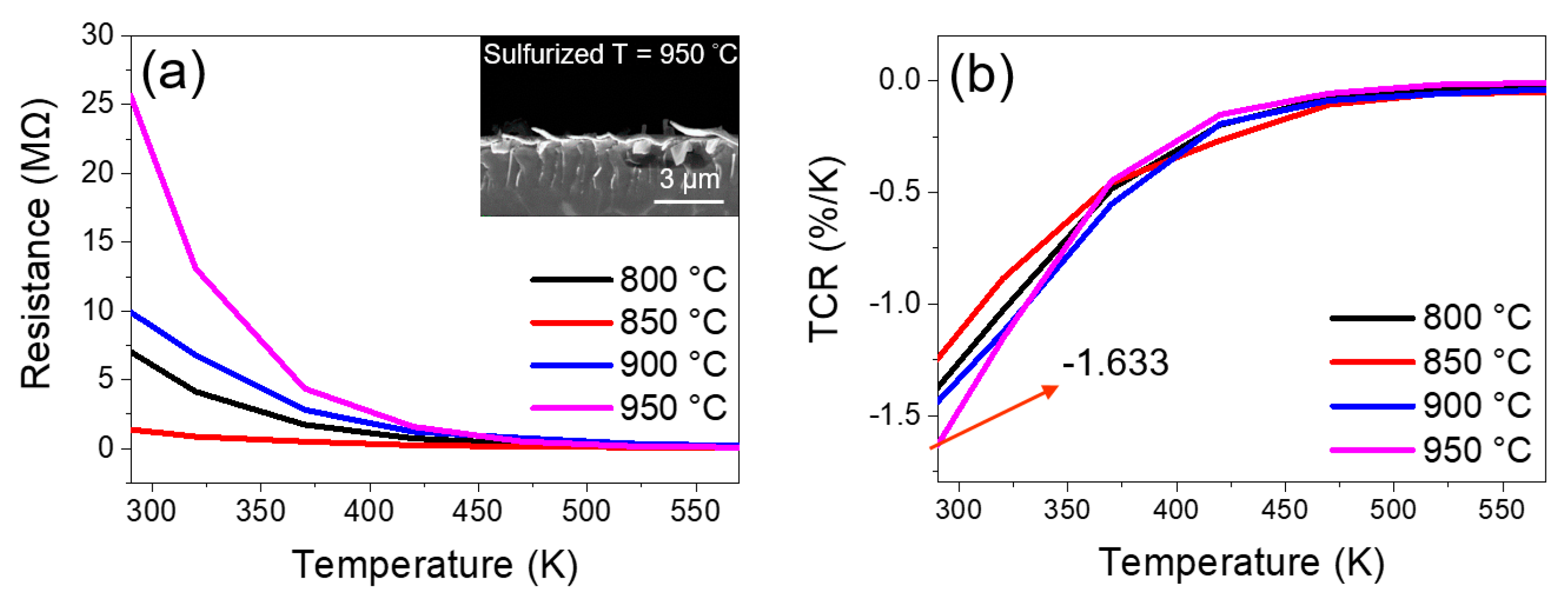
In order to understand the possibility of applying MoxW1−xS2 thin films as thermal sensors, we measured the temperature-dependent I–V characteristics of our samples from 290 to 570 K, as shown in Figure 4a–d. The distance (ca. 5 mm) between the prepared electrodes was maintained as constant as possible for each sample. The I–V results show linear and ohmic measurements within −1 to 1 V for each sample at various temperatures. The resistance trend for each sample was consistent with that of the semiconductor, decreasing with increasing measured temperature. The reason is that the electron absorbed the thermal energy when the temperature increased and further broke covalent bond to become a free electron. More and more free electrons were produced as the temperature increased, resulting in increased conduction and decreased resistance.
According to Ohm’s law, we calculated the resistances in terms of the results in Figure 4a–d. The resistances of the samples measured at different temperatures are shown in Figure 5a. The relationship between resistance and structural properties for a sample is worth investigating, especially at measurements of 290 K, which is close to room temperature. Figure 5a shows that the resistance was about 7, 1.3, 9.9, and 25.6 MΩ when the sample was sulfurized at 800, 850, 900, and 950 °C, respectively. The above SEM and XRD results suggest that the sample sulfurized at 800 °C had an obvious amorphous structure, which led to its slightly higher resistance in comparison with the sample sulfurized at 850 °C. However, as increasing the sulfurizing temperature improved the crystal quality of the sample, the porous feature would be a critical reason for increasing the resistance of the MoxW1−xS2 thin film. The highest resistance value of 25.6 MΩ could be attributed to the severe interface separation between the MoxW1−xS2 thin film and the substrate due to large stress when the sample was sulfurized at 950 °C. The cross-section SEM image reveals these sheet-like MoxW1−xS2 thin films were partially detached. We also calculated the TCR of each sample from Figure 5a using Equation (1) [11,12]:
where R0 is the resistance of each sample at 290 K. Figure 5b displays the TCR values of the samples measured at different temperatures. In comparison with the TCR values (0.29% to 0.48%) for metallic the MoW alloy obtained by Geiss et al. [23], the MoxW1−xS2 thin film sulfurized at 950 °C had a TCR value of −1.633%/K. Kato et al. reported that any degradation in crystal quality would lower the TCR of a semiconductor [24]. Moreover, a well-crystalized structure can result in a high TCR for a VO2 thin film [25]. So far, no relevant study reports the correlations between crystal quality and TCR for the MoxW1−xS2 compound. Therefore, our results show that a well-crystalized MoxW1−xS2 thin film has a high TCR, which is beneficial for its application in thermal sensors.
4. Conclusions
In this study, we deposited a MoW alloy on a Si substrate using a sputter system. Consequently, we successfully sulfurized the MoW alloy from 800 to 950 °C, forming MoxW1−xS2 ternary compound films, which was confirmed by Raman spectra results. Both the SEM and XRD results indicated that increasing sulfurization temperature improved the crystal structure and produced further changes in microstructures to affect the resistance and TCR for the MoxW1−xS2. The I–V results showed that the well-crystalized MoxW1−xS2 thin film sulfurized at 950 °C had a high TCR of −1.633%/K. This attractive high TCR of the MoxW1−xS2 thin film demonstrates its potential for its further development and future applications in thermal sensors.
Author Contributions
Data curation, T.-S.K. and E.-T.L.; Formal analysis, T.-S.K.; Funding acquisition, Y.-L.Y.; Investigation, T.-S.K. and E.-T.L.; Methodology, T.-S.K., E.-T.L., X.-W.H. and Y.-L.Y.; Project administration, T.-S.K., P.-T.W. and Y.-L.Y.; Resources, T.-S.K. and Y.-L.Y.; Software, E.-T.L.; Supervision, T.-S.K.; Writing—original draft, T.-S.K.; Writing—review & editing, T.-S.K. All authors have read and agreed to the published version of the manuscript.
Funding
This research was funded by the Ministry of Science and Technology of Taiwan (grant number: MOST 110-2221-E-017-009 and MOST 109-2221-E-018-012).
Institutional Review Board Statement
Not applicable.
Informed Consent Statement
Not applicable.
Data Availability Statement
Data are contained within the article.
Acknowledgments
The authors thank J.-Y. Chen (National Chung Hsing University) for assistance with Raman instrumentation and for the useful discussions.
Conflicts of Interest
The authors declare no conflict of interest.
References
- Wang, Q.H.; Kalantar-Zadeh, K.; Kis, A.; Coleman, J.N.; Strano, M.S. Electronics and optoelectronics of two-dimensional transition metal dichalcogenides. Nat. Nanotechnol. 2012, 7, 699–712. [Google Scholar] [CrossRef] [PubMed]
- Wang, H.; Yu, L.; Lee, Y.H.; Shi, Y.; Hsu, A.; Chin, M.L.; Li, L.J.; Dubey, M.; Kong, J.; Palacios, T. Integrated circuits based on bilayer MoS2 transistors. Nano Lett. 2012, 12, 4674–4680. [Google Scholar] [CrossRef] [PubMed] [Green Version]
- Jo, S.; Ubrig, N.; Berger, H.; Kuzmenko, A.B.; Morpurgo, A.F. Mono- and bilayer WS2 light-emitting transistors. Nano Lett. 2014, 14, 2019–2025. [Google Scholar] [CrossRef] [PubMed] [Green Version]
- Yang, W.; Shang, J.; Wang, J.; Shen, X.; Cao, B.; Peimyoo, N.; Zou, C.; Chen, Y.; Wang, Y.; Cong, C.; et al. Electrically Tunable Valley-Light Emitting Diode (vLED) Based on CVD-Grown Monolayer WS2. Nano Lett. 2016, 16, 1560–1567. [Google Scholar] [CrossRef] [PubMed]
- Tan, H.; Fan, Y.; Zhou, Y.; Chen, Q.; Xu, W.; Warner, J.H. Ultrathin 2D Photodetectors Utilizing Chemical Vapor Deposition Grown WS2 with Graphene Electrodes. ACS Nano 2016, 10, 7866–7873. [Google Scholar] [CrossRef]
- Shokri, A.; Salami, N. Gas sensor based on MoS2 monolayer. Sens. Actuators B Chem. 2016, 236, 378–385. [Google Scholar] [CrossRef]
- Xu, X.; Luo, F.; Tang, W.; Hu, J.; Zeng, H.; Zhou, Y. Enriching Hot Electrons via NIR-Photon-Excited Plasmon in WS2 @Cu Hybrids for Full-Spectrum Solar Hydrogen Evolution. Adv. Funct. Mater. 2018, 28, 1804055. [Google Scholar] [CrossRef]
- Xu, X.; Luo, F.; Zhou, G.; Hu, J.; Zeng, H.; Zhou, Y. Self-assembly optimization of cadmium/molybdenum sulfide hybrids by cation coordination competition toward extraordinarily efficient photocatalytic hydrogen evolution. J. Mater. Chem. A 2018, 6, 18396–18402. [Google Scholar] [CrossRef]
- Ma, J.; Yuan, Y.; Sun, P. Performances enhancement of graphene/n-Si Schottky junction solar cells with dual-functional MoS2 interfacial layers. J. Alloys Compd. 2021, 883, 160898. [Google Scholar] [CrossRef]
- Krishnamoorthy, D.; Prakasam, A. Graphene Hybridized with Tungsten disulfide (WS2) Based Heterojunctions Photoanode Materials for High Performance Dye Sensitized Solar Cell Device (DSSCs) Applications. J. Clust. Sci. 2020, 32, 621–630. [Google Scholar] [CrossRef]
- Khan, A.I.; Khakbaz, P.; Brenner, K.A.; Smithe, K.K.H.; Mleczko, M.J.; Esseni, D.; Pop, E. Large temperature coefficient of resistance in atomically thin two-dimensional semiconductors. Appl. Phys. Lett. 2020, 116, 203105. [Google Scholar] [CrossRef]
- Lee, M.; Mazaheri, A.; van der Zant, H.S.J.; Frisenda, R.; Castellanos-Gomez, A. Drawing WS2 thermal sensors on paper substrates. Nanoscale 2020, 12, 22091–22096. [Google Scholar] [CrossRef] [PubMed]
- Daoudi, K.; Tsuchiya, T.; Yamaguchi, I.; Manabe, T.; Mizuta, S.; Kumagai, T. Microstructural and electrical properties of La0.7Ca0.3MnO3 thin films grown on SrTiO3 and LaAlO3 substrates using metal-organic deposition. J. Appl. Phys. 2005, 98, 013507. [Google Scholar] [CrossRef]
- Ko, T.S.; Chen, Y.L. Hybrid Enhancement of Surface-Enhanced Raman Scattering Using Few-Layer MoS2 Decorated with Au Nanoparticles on Si Nanosquare Holes. Nanomaterials 2022, 12, 786. [Google Scholar] [CrossRef] [PubMed]
- Li, H.; Zhang, Q.; Yap, C.C.R.; Tay, B.K.; Edwin, T.H.T.; Olivier, A.; Baillargeat, D. From Bulk to Monolayer MoS2: Evolution of Raman Scattering. Adv. Funct. Mater. 2012, 22, 1385–1390. [Google Scholar] [CrossRef]
- Zhao, W.; Ghorannevis, Z.; Amara, K.K.; Pang, J.R.; Toh, M.; Zhang, X.; Kloc, C.; Tan, P.H.; Eda, G. Lattice dynamics in mono- and few-layer sheets of WS2 and WSe2. Nanoscale 2013, 5, 9677–9683. [Google Scholar] [CrossRef] [Green Version]
- Lin, Z.; Thee, M.T.; Elías, A.L.; Feng, S.; Zhou, C.; Fujisawa, K.; Perea-López, N.; Carozo, V.; Terrones, H.; Terrones, M. Facile synthesis of MoS2 and MoxW1-xS2 triangular monolayers. APL Mater. 2014, 2, 092514. [Google Scholar] [CrossRef] [Green Version]
- Chen, Y.; Xi, J.; Dumcenco, D.O.; Liu, Z.; Kazu, S.; Wang, D.; Shuai, Z.; Huang, Y.; Xie, L. Tunable Band Gap Photoluminescence from Atomically Thin Transition-Metal Dichalcogenide Alloys. ACS Nano 2013, 7, 4610–4616. [Google Scholar] [CrossRef]
- Park, J.; Kim, M.S.; Park, B.; Oh, S.H.; Roy, S.; Kim, J.; Choi, W. Composition-Tunable Synthesis of Large-Scale Mo1-xWxS2 Alloys with Enhanced Photoluminescence. ACS Nano 2018, 12, 6301–6309. [Google Scholar] [CrossRef]
- Liang, K.; Chianelli, R.; Chien, F.; Moss, S. Structure of poorly crystalline MoS2—A modeling study. J. Non-Cryst. Solids 1986, 79, 251–273. [Google Scholar] [CrossRef]
- Duphil, D.; Bastide, S.; Rouchaud, J.C.; Pastol, J.L.; Legendre, B.; Lévy-Clément, C. The chemical synthesis in solution and characterization of transition metal dichalcogenide MX2 (M = Mo, W; X = S, Se) nanoparticles. Nanotechnology 2004, 15, 828–832. [Google Scholar] [CrossRef]
- Chang, L.; Yang, H.; Fu, W.; Zhang, J.; Yu, Q.; Zhu, H.; Chen, J.; Wei, R.; Sui, Y.; Pang, X.; et al. Simple synthesis of MoS2 inorganic fullerene-like nanomaterials from MoS2 amorphous nanoparticles. Mater. Res. Bull. 2008, 43, 2427–2433. [Google Scholar] [CrossRef]
- Geiss, W.; Liempt, J.A.M.V. Zur Kenntnis des binären Systems Wolfram-Molybdän. Z. Anorg. Allg. Chem. 1923, 128, 355–360. [Google Scholar] [CrossRef]
- Kato, K.; Ono, T. Change in Temperature Coefficient of Resistance of Heavily Doped Polysilicon Resistors Caused by Electrical Trimming. Jpn. J. Appl. Phys. 1996, 35, 4209–4215. [Google Scholar] [CrossRef]
- Li, J.; Yuan, N. Temperature sensitivity of resistance of VO2 polycrystalline films formed by modified ion beam enhanced deposition. Appl. Surf. Sci. 2004, 233, 252–257. [Google Scholar] [CrossRef]
Figure 1.
Raman spectra of the MoxW1−xS2 thin films by sulfurizing MoW alloy at different temperatures from 800 to 950 °C.
Figure 1.
Raman spectra of the MoxW1−xS2 thin films by sulfurizing MoW alloy at different temperatures from 800 to 950 °C.

Figure 2.
SEM images of the MoxW1−xS2 thin films by sulfurizing MoW alloy at different temperatures: (a) 800, (b) 850, (c) 900, and (d) 950 °C. The insertion in each figure is the corresponding cross sectional SEM image.
Figure 2.
SEM images of the MoxW1−xS2 thin films by sulfurizing MoW alloy at different temperatures: (a) 800, (b) 850, (c) 900, and (d) 950 °C. The insertion in each figure is the corresponding cross sectional SEM image.

Figure 3.
XRD 2θ scan results of the MoxW1−xS2 thin films sulfurized at various temperatures.

Figure 4.
The temperature-dependent I–V characteristics of the MoxW1−xS2 thin films sulfurized at (a) 800, (b) 850, (c) 900, and (d) 950 °C.
Figure 4.
The temperature-dependent I–V characteristics of the MoxW1−xS2 thin films sulfurized at (a) 800, (b) 850, (c) 900, and (d) 950 °C.

Figure 5.
(a) The resistance as a function of measured temperature for the MoxW1−xS2 thin films sulfurized at various temperatures. The insert shows a cross-section SEM image of the MoxW1−xS2 thin film sulfurized at 950 °C. (b) The corresponding TCR values of the samples obtained from (a).
Figure 5.
(a) The resistance as a function of measured temperature for the MoxW1−xS2 thin films sulfurized at various temperatures. The insert shows a cross-section SEM image of the MoxW1−xS2 thin film sulfurized at 950 °C. (b) The corresponding TCR values of the samples obtained from (a).

Publisher’s Note: MDPI stays neutral with regard to jurisdictional claims in published maps and institutional affiliations. |
© 2022 by the authors. Licensee MDPI, Basel, Switzerland. This article is an open access article distributed under the terms and conditions of the Creative Commons Attribution (CC BY) license (https://creativecommons.org/licenses/by/4.0/).
Share and Cite
MDPI and ACS Style
Ko, T.-S.; Lin, E.-T.; Huang, X.-W.; Wu, P.-T.; Yang, Y.-L. High-Temperature Coefficient of Resistance in MoxW1−xS2 Thin Film. Appl. Sci. 2022, 12, 5110. https://0-doi-org.brum.beds.ac.uk/10.3390/app12105110
AMA Style
Ko T-S, Lin E-T, Huang X-W, Wu P-T, Yang Y-L. High-Temperature Coefficient of Resistance in MoxW1−xS2 Thin Film. Applied Sciences. 2022; 12(10):5110. https://0-doi-org.brum.beds.ac.uk/10.3390/app12105110
Chicago/Turabian StyleKo, Tsung-Shine, En-Ting Lin, Xin-Wen Huang, Po-Tang Wu, and Yi-Lin Yang. 2022. "High-Temperature Coefficient of Resistance in MoxW1−xS2 Thin Film" Applied Sciences 12, no. 10: 5110. https://0-doi-org.brum.beds.ac.uk/10.3390/app12105110
Note that from the first issue of 2016, this journal uses article numbers instead of page numbers. See further details here.