1. Introduction
Ge incorporation into the kesterite (Cu
2ZnSnSe
4) system in order to form Cu
2Zn(Sn,Ge)Se
4 (CZTGSe) material is considered to be a promising approach for obtaining photovoltaic absorbers with a higher and tunable band gap in the range of 1.0 eV to 1.5 eV [
1,
2]. In addition, Ge is known to occupy the Sn sites, possibly reducing or passivating Sn-related deep defects, i.e., V
Sn, Sn
Zn and Cu
Sn, which are assumed to be a major cause of high
VOC deficits in kesterite [
3,
4,
5,
6,
7]. Commonly reported approaches for Ge incorporation into kesterites are based on the inclusion of Ge in the precursor layer, which can be grown by spray coating, electrodeposition and sputtering [
2,
8,
9,
10]. It has been reported that such approaches can lead to the localized incorporation of Ge [
6], significant variation in grain size [
8] and inferior device performance, which can be improved by ambient storage [
2]. However, most of the reported processes have in common that they are based on processes that were previously optimized for a Ge-free-material system. As a consequence of adding Ge to the precursor, the entire alloy configuration, distribution of elements, and overall composition ratios in the precursor are changed, altering the reaction pathway for the kesterite-phase formation. In such a case, a well-optimized process for Ge-free-kesterite growth may need further optimization steps for Ge incorporation. The precursor structure and further process parameters may need a full re-optimization or even significant modifications to avoid the formation of other secondary phases and further undesirable defects.
Here we report an approach in which we avoid the aforementioned problems by using an alternative method to incorporate Ge into the layer after the high-temperature phase of the selenization process, thereby maintaining the previously optimized precursor structure and the main formation pathway identical to the Ge-free growth process. In brief, the Ge is incorporated into the already-formed kesterite-absorber layer via the vapor phase during the high-temperature phase of the selenization process. During this step the composition of the layer is usually shifted from Cu-rich to Cu-poor [
11,
12]. Since the main kesterite phase formation route is unaltered, the process offers high reproducibility in terms of layer morphology and targeted final-layer composition. The Ge-based devices show slightly lower efficiencies and could reach the range of 10%, which is slightly below the as-grown efficiencies of Ge-free devices. However, investigations into long-term device stability indicate an improvement of the long-term performance by adding Ge to kesterite solar cells.
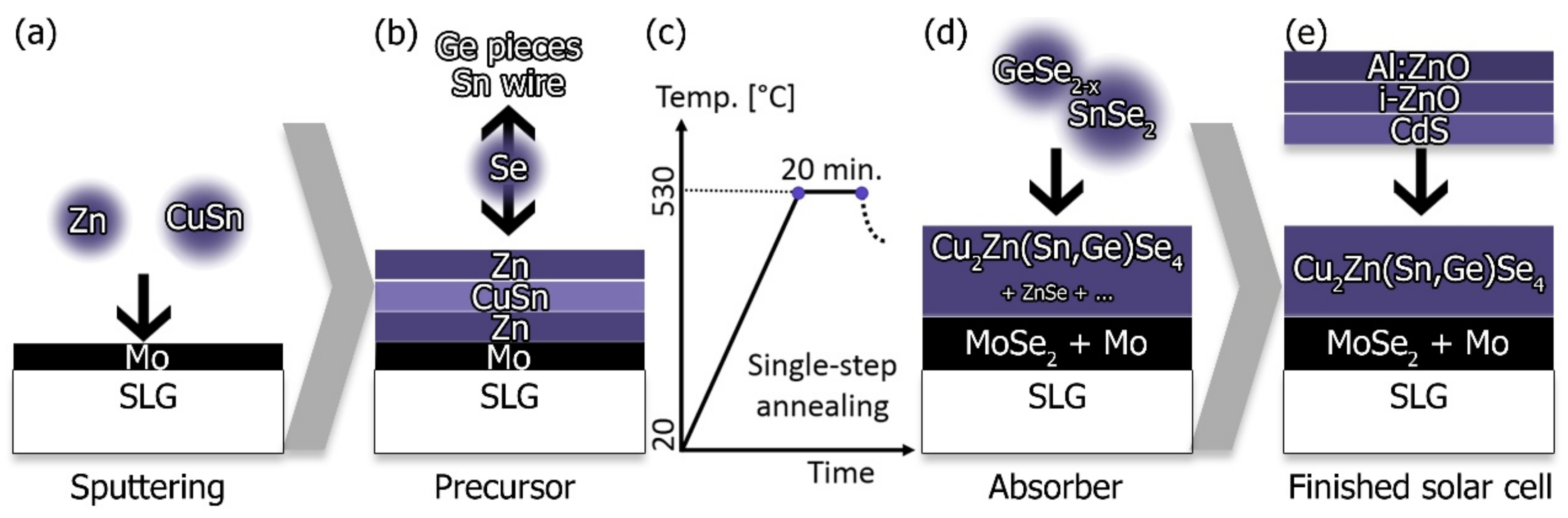
2. Materials and Methods
CZTSe and CZTGSe absorbers were prepared by the one-step selenization of stacked elemental and alloyed precursor layers (Zn/Cu-Sn/Zn). The samples were produced on 3 mm soda-lime glass (SLG) coated with two 250 nm Mo layers and treated with Ar plasma (in a von Ardenne cluster tool) for 3 min before being cut into the desired size of 25 mm by 25 mm, and one more minute of direct treatment (and without leaving the vacuum) before sputtering the metallic-precursor layer (von Ardenne cluster tool). The Ar-plasma-etching steps were performed in order to remove oxides and organic residues from the surface. The substrates were provided by ZSW (Zentrum für Sonnenenergie und Wasserstofforschung Baden-Württemberg) as well as Manz AG. The Zn/Cu-Sn/Zn precursor stack was prepared by using the sputter durations of 324 s, 1625 s, and 44 s, respectively. The sputtering rates were estimated from a sputtering process of long duration over a large area and were approximately 23.7 μgs
−1cm
−2 for Zn and 11.1 μgs
−1cm
−2 for the Cu-Sn layer of the mixed target [
13]. Annealing was performed in a semi-closed graphite susceptor (a.k.a. graphite box) inside a conventional quartz-glass tube furnace (Carbolite Eurotherm 2416CG, 2416P8) by following the same process parameters as previously reported for our Ge-free-reference process, i.e., pump and purge cycles under N
2, 10 mbar base pressure, a heating ramp of 10 °C/min, 20 min dwelling time upon reaching a temperature of 530 °C [
12,
14]. Two identical graphite boxes were used to maintain one “clean” box for the Ge-free-reference process. The graphite boxes could hold two samples for simultaneous processing, and had pockets on each side of the samples for the even distribution of Se pellets, Sn wire, and Ge flakes. The amount and purities of the added reactants were 210 ± 2 mg of Se pellets (Mateck, 5N purity), 37.0 ± 0.4 mg of Sn wire (AlfaAesar, 4N purity, i.e., 10.0 ± 0.1 cm wire with 0.25 mm diameter) and, depending on the desired Ge addition, between 0 mg (reference process) and 110 ± 5 mg of Ge flakes (AlfaAesar, 5N purity). The reference process for synthesizing Ge-free absorbers is described in more detail elsewhere [
11,
12,
13]. In brief, the Cu-rich and alloyed precursor layer (Zn/Cu-Sn/Zn) is annealed in presence of elemental Sn wire and Se pellets in a semi-closed graphite box. During the high-temperature stage of the annealing process (i.e., at
T = 530 °C), SnSe
2−x vapor (from the selenized Sn wire) incorporates into the layer, which then shifts towards a Cu-poor composition. This reference process was adapted in order to incorporate Ge into the absorber layer. Adding Ge (in addition to the Sn wire) to the presented approach was expected to yield a similar composition shift towards a Cu-poor composition due to the simultaneous supply of GeSe
2−x and SnSe
2−x vapor to the sample surface. GeSe
2−x has a higher vapor pressure [
15,
16,
17,
18] (see
Figure S1), and can thus reach the samples earlier (already at lower temperatures) than SnSe
2−x. The resulting absorbers were approximately (1.5 ± 0.5) μm in thickness.
The fabricated CZTSe and CZTGSe absorbers were subsequently coated with a CdS-buffer layer by chemical-bath deposition (solution containing cadmium acetate, ammonia, and thiourea [
14,
19]) for 10 min at 70 °C resulting in an approximately 50 nm CdS layer. 75 nm of i-ZnO and 500 nm of Al:ZnO (RF-sputtered, von Ardenne cluster tool) were added afterwards to finish the solar-cell device, as shown in
Figure 1. No anti-reflective coating or metallic contact grid was applied to any of the samples presented here. Sample contacting was performed by exposing the Mo layer and placing two Indium dots for the back contacting. The front contacting was established by carefully placing probe heads directly on the ZnO. Each sample was divided into nine smaller cells by mechanical scribing, resulting in laboratory-scale cells of approximately 5 mm by 5 mm.
The final absorber compositions were determined by cross-calibrated (except for Ge content) energy-dispersive X-ray spectroscopy (EDX) measurements (FEI Helios 600i). An averaging of three independent and randomly positioned measurements was performed per sample. EDX surface mappings and EDX cross-section mappings of cleaved samples were performed for analysis of the elemental distribution. Shallow-angle-focused ion-beam milling was performed on some samples to investigate the depth-resolved element distributions (FEI Helios 600i), which is described in more detail in [
11]. Raman measurements were performed with the laser wavelengths 532 nm and 457 nm (LabRAM Aramis Horiba). IV measurements under standard test conditions on each solar cell were performed using an AAA-class sun simulator (Photo Emission Tech Inc., USA). External-quantum-efficiency (EQE) measurements were taken at room temperature with a spectral range of 300 nm to 1400 nm (Bentham TMc300 Monochromator, lamps from Bentham instruments Ltd., ILD 75E QH chop, Xenon and Quartz-Halogen, Stanford research systems SR 830 DSP lock-in amplifier). The band gap
EG of the absorber was extracted by performing a linear extrapolation of EQE² over the energy
E. Urbach energies
EU were obtained by linearly fitting ln(EQE) as a function of the
E of the exponential tail below the band gap edge [
20,
21]. The presented values for the
VOC deficit are given relative to the Shockley–Queisser limit according to the empiric Equation (1) [
2,
22,
23]
where
EG is the band gap extracted from EQE,
q is the elementary charge and
VOC is the open-circuit voltage obtained from IV measurements. Accelerated-aging tests were performed in a climate chamber (Weiss Umwelttechnik GmbH, type SC 600/70) at a temperature of 85 °C and relative humidity of 20%. The samples were placed in petri dishes covered with lids to protect the samples from any possible water-droplet condensation in the chamber.
3. Results and Discussion
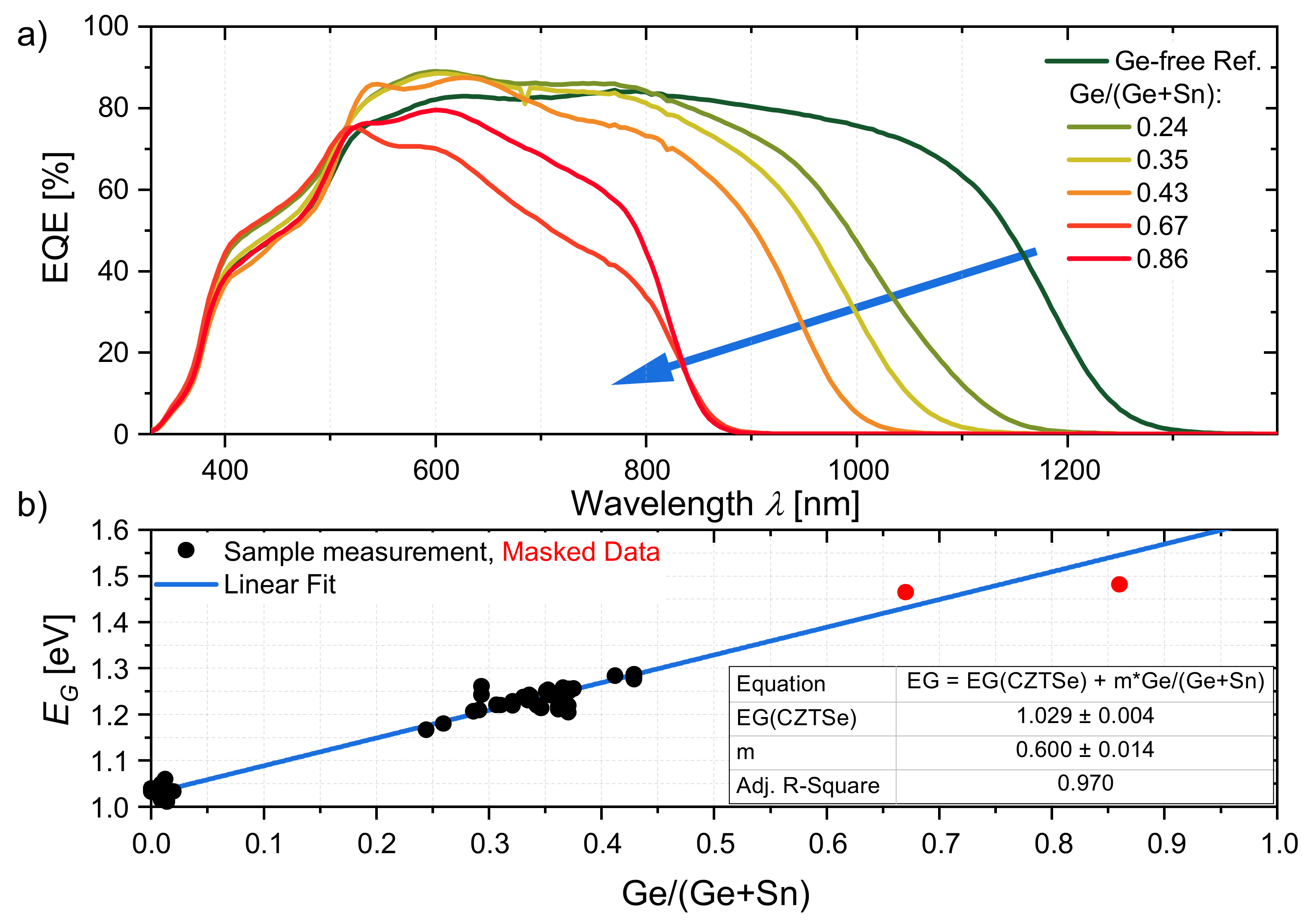
The effective incorporation of Ge into the kesterite absorber is shown in
Figure 2 by the EDX results along with the EQE spectra and the
EG values extracted from them. By varying the added Ge amount, CZTGSe-absorber layers with Ge/(Ge + Sn) ratios in the range of 0.0 to 0.86 were synthesized. For better viewing, only a few selected EQE spectra covering the discussed range are shown in
Figure 2a; band gap values extracted from the full set of available EQE spectra are shown in
Figure 2b as a function of the Ge content.
We find a clear shift in the absorber band gap towards higher energies with increasing Ge content, showing the expected linear behavior for the samples with Ge/(Ge + Sn) < 0.67. The slope of this relation amounts to (0.600 ± 0.014) eV per Ge/(Ge + Sn), which is close to the value of 0.52 reported in the literature for other growth techniques [
1,
2]. For higher Ge contents, i.e., ≥ 0.67, further increased Ge content in the layer does not lead to the expected band gap rise, indicating that the incorporation of Ge into the kesterite crystal may have reached a saturation point, above which the further addition of Ge may rather lead to condensation, secondary phases, or crystal defects. In this region, major losses, which are predominant in the high wavelength part of the presented EQE spectra, are visible, indicating the presence of transport issues, increased recombination, and reduced collection lengths [
2].
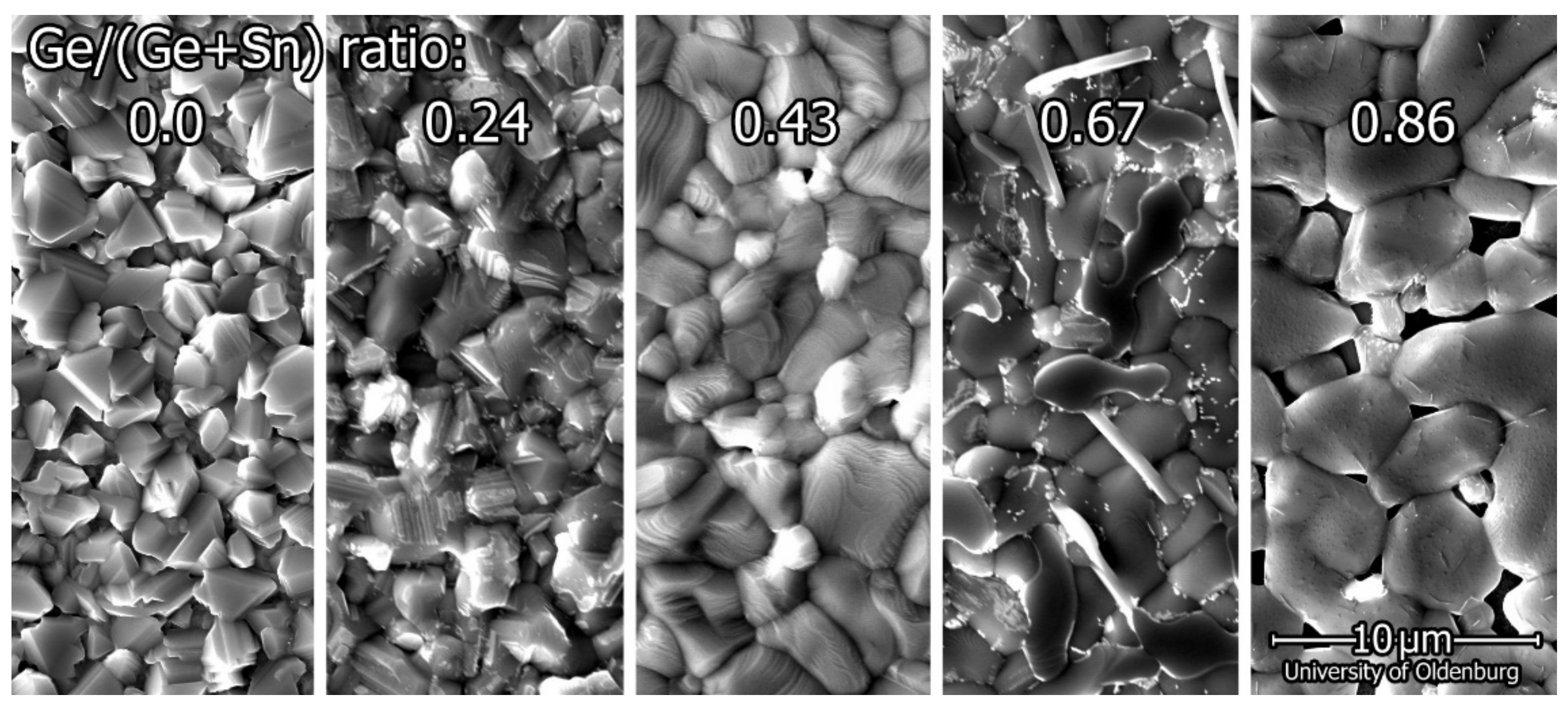
The morphology of the samples was influenced by the added Ge content as shown in
Figure 3. The morphology of the reference sample shows sharp grains with sizes of approximately 2 μm. Samples with added Ge show a clear trend towards larger grains and less sharp edges. The most extreme sample with Ge/(Ge + Sn) = 0.86 shows grain sizes of approximately 5–6 μm. With increased grain size the density of the grain boundaries decreases, which could influence the recombination behavior. Overall, the possible effects of grain size are assumed to be overlapped by other effects (e.g., secondary phases, strain, etc.); therefore, within this study no conclusions were drawn about the possible influence of grain size on the device performance.
The SEM top-view images in
Figure 3 show the formation of rod-shaped particles on top of the samples with Ge/(Ge + Sn) ≥ 0.67. Using Raman measurements on the surface, these particles were identified as SnSe. For the performance of a depth-dependent phase analysis, a shallow-angle cross section was created using focused ion-beam milling [
24]. The Raman and EDX measurements of the wedge-shaped cross section revealed that the SnSe secondary phase was occurring throughout the full depth of the absorber layer (see
Figure S2). Interestingly, the sample with Ge/(Ge + Sn) ratio of 0.86 did not show clear SnSe secondary phases; however, large voids between the grains were observed, possibly indicating an evaporation of volatile secondary phases formed in the process (e.g., SnSe
2−x and GeSe
2−x).
Considering sample homogeneity, morphology and EQE characteristics, the developed process therefore seems suitable for synthesizing CZTGSe-absorber layers with low to intermediate amounts of Ge (i.e., Ge/(Ge + Sn) ≤ 0.43), which appears to be more than sufficient to cover the composition range for highest expected device performance reported in the literature [
2,
8,
25]. The discussion in the following section is therefore focused on the samples with Ge/(Ge + Sn) ≤ 0.43.
According to our previous work on Ge-free-kesterite devices [
11,
12], the CZTSe phase forms below a temperature of 400 °C in the presence of secondary phases (e.g., ZnSe and Cu
2Se). At higher temperatures, the SnSe
2−x vapor from the supplied Sn wire in the graphite susceptor incorporates into the layer, leading to further growth of the CZTSe phase by reacting with ZnSe and Cu
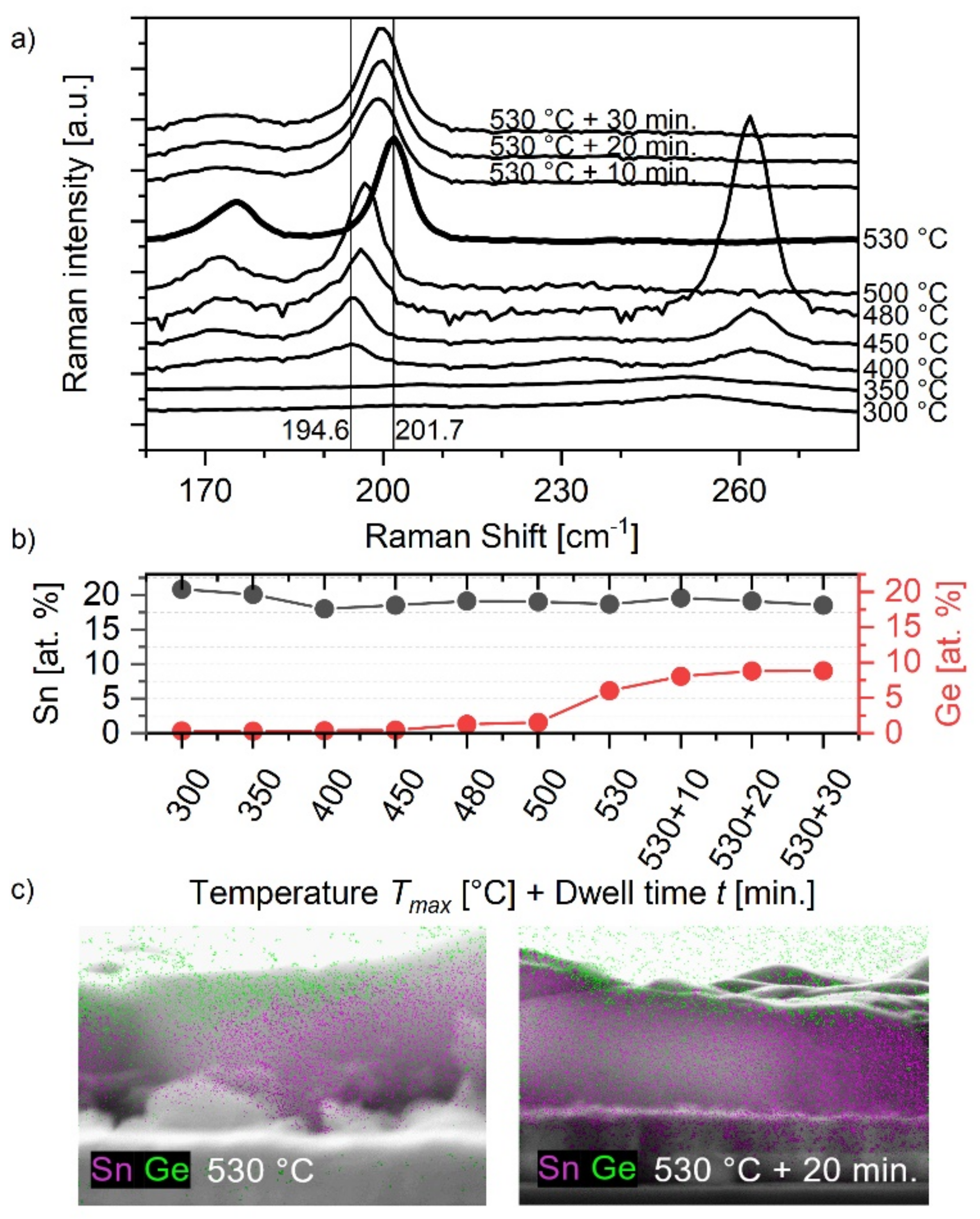
2Se, leading to a composition shift (Cu-rich to Cu-poor). To understand the formation path and the composition shift in the Ge-containing process, a series of interrupted-annealing experiments was performed. The selenization process was interrupted at different temperatures by quenching with nitrogen gas. Raman and EDX analyses were carried out on the samples and the results are summarized in
Figure 4a,b.
Up to 400 °C, the process is expected to behave identical to our reference Ge-free kesterite process. No significant amount of Ge was found in the layer (Ge/(Ge + Sn) < 0.02) and the A1 mode is centered at wavenumbers below 196 cm
−1, indicating no presence of Ge in the CZTSe phase [
26]. After reaching the annealing temperature of 480 °C, the first indications of Ge incorporation were observed. Raman shows a shift of the A1 mode from 194.6 cm
−1 at 430 °C to 196.3 cm
−1 at 480 °C and the EDX measurements show a ratio of Ge/(Ge + Sn) ≈ 0.06. Once the temperature reaches 500 °C, Raman peaks related to secondary phases disappear (as described above for the reference process [
11,
12], here shown Cu
2-xSe at 263 cm
−1 [
27,
28]), the A1 mode shifts further to 196.8 cm
−1 and the Ge content (from EDX) further increases (Ge/(Ge + Sn) ≈ 0.07). At 530 °C, the largest A1 mode shift of 201.7 cm
−1 is observed, which would correspond to a Ge content of Ge/(Ge + Sn) ≈ 0.56 (see
Figure S3). However, the corresponding Ge content observed from EDX measurements only amounted to Ge/(Ge + Sn) ≈ 0.24. The possible reason for this significant discrepancy could be a higher Ge concentration at the surface region of the layer detected by Raman, which is more surface sensitive than EDX [
8]. For the samples with a dwell time of 10 min and longer, the A1 mode shifts back towards lower wavenumbers, i.e., 199.4 ± 0.3 cm
−1, and the peak position matches again with the EDX measured Ge concentration (Ge/(Ge + Sn) ≈ 0.30) (see
Figure S3). To investigate the possibility of a composition gradient in the sample from the interruption experiment, we performed cross-sectional EDX mappings of the sample corresponding to 530 °C (quenched), and 530 °C with 20 min of dwell time (normal procedure).
Figure 4c shows the Sn and Ge distribution across the depth of these samples, exhibiting higher accumulation of Ge on the surface of the layer for the interrupted sample (
Figure 4c, left hand side). The sample with dwell time shows intermixed Ge and Sn throughout the depth of the absorber (
Figure 4c, right hand side). This result confirms the previously discussed observation from Raman and EDX and illustrates the formation and decay of an initial front-surface Ge gradient during this process. We note that the Sn content in the layer stays constant throughout all the samples. The overall composition shifted from a Cu-rich start to a Cu-poor (& Zn-rich) absorber during the process due to GeSe incorporation (see
Figure S4).
The ex-situ Raman and EDX measurements suggest that the Ge incorporation into kesterite does not significantly influence the reported formation path of the kesterite phase [
11,
12]. In the case of Ge incorporation, the Cu-rich to Cu-poor composition shift occurs at a slightly lower temperature (480 °C to 530 °C) due to the higher vapor pressure of GeSe
2−x as compared to SnSe
2−x (see
Figure S1). This means that up to this temperature the process is unaltered and all reaction steps and pre-steps of the kesterite formation are not influenced.
We note that XRD measurements of selected samples further confirms that no significant Ge incorporation is observed until 450 °C. XRD measurements show no signature peaks corresponding to the SnSe
2−x and GeSe
2−x phases (
Figure S5 and description).
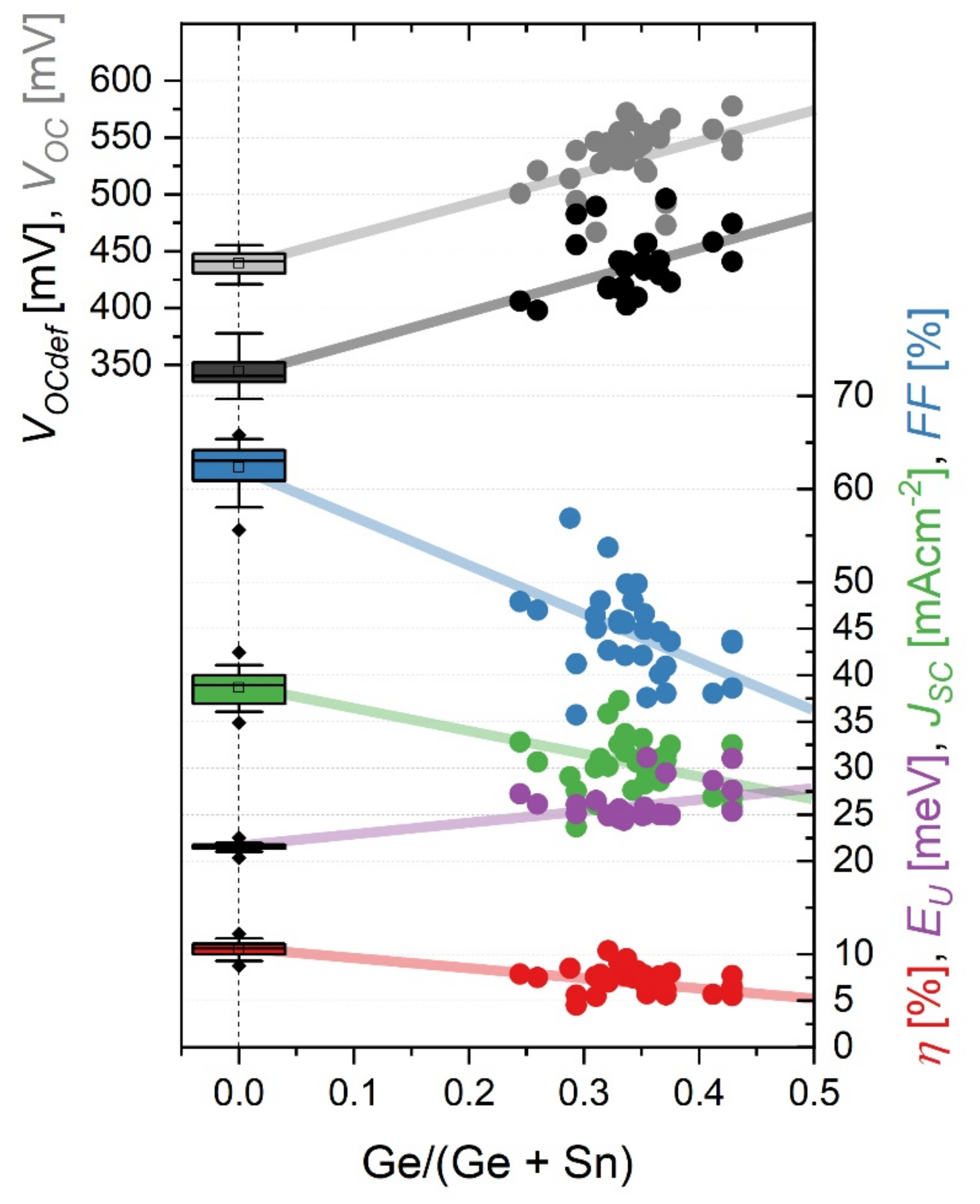
To measure the PV device characteristics, all the samples were coated with CdS and TCO layers to fabricate the solar cells. A summary of IV parameters and EQE analysis for samples with Ge/(Ge + Sn) ≤ 0.43 is given in
Figure 5.
As expected, the open-circuit voltage
VOC is increased, and the short-circuit current
JSC drops due to the increased band gap (see
Figure 2). However, the
VOC deficit follows the trend of the
Voc, showing that the increased band gap of the absorber is only partially converted into an open-circuit voltage gain. The magnitude of the
VOC deficit, commonly attributed to Sn-related deep defects, remains unaffected by the approach in our study.
The Urbach energy
EU, extracted from the EQE spectra, describes the magnitude of the band tailing and is considered as an indicator of crystal quality [
29,
30]. A clear difference between
EU of the reference and Ge-containing samples is visible. This can be explained by an increase in the general crystal disorder by adding an extra element to the crystal structure in the case of Ge-containing kesterite.
The fill factor
FF of all CZTGSe devices was found to be lower than the reference CZTSe. A possible reason for this could be the non-adapted solar-cell-device-processing steps. These were only optimized for the Ge-free kesterite and simplified for a facile procedure that contains no treatments besides the main steps (i.e., no air annealing, no etching, etc.). In the case of Ge-containing kesterite, additional steps such as etching or pre-treatment for the buffer-layer deposition might be necessary to improve the CdS homogeneity and quality of the interface in order to overcome the loss in the observed fill factors. The noticeable scattering of the data shown in
Figure 5 is due to process variations over a longer time range (months), different substrate batches and different CdS deposition batches. The overall PCE
η for CZTGSe cells is lower than the Ge-free-CZTSe reference, yet still shows one of the highest reported efficiencies of 10.4%, with a Ge/(Ge + Sn) ratio of 0.32 (
EG = 1.22 eV). The IV curves of the corresponding sample are shown in
Figure S6. IV curves for the five different Ge ranges introduced in the context of
Figure 3 are compared in
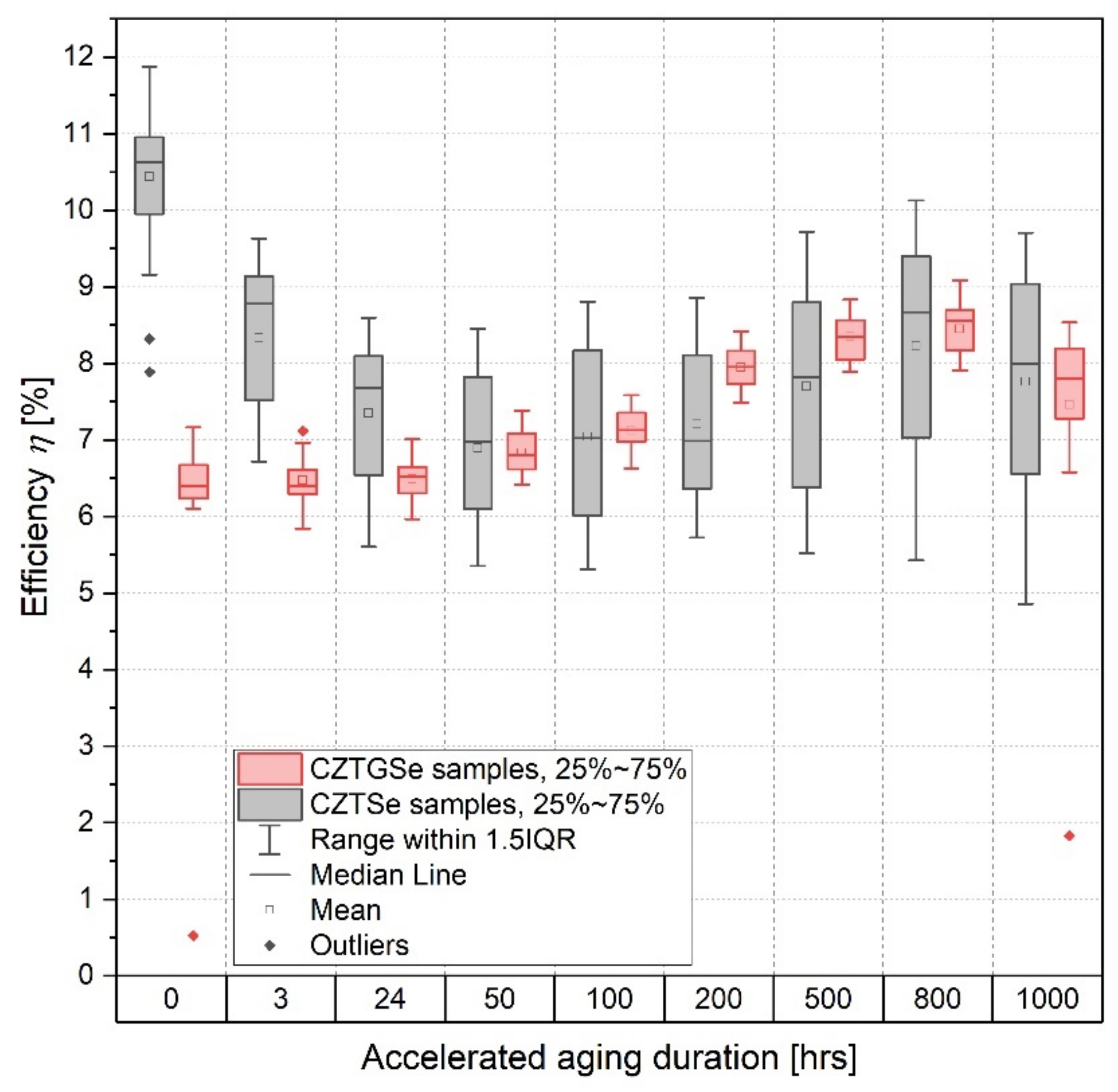
Figure S7. In addition to the IV and EQE measurements of freshly fabricated devices, a time-stability analysis was performed using an accelerated-aging procedure. A total of 12 CZTSe solar cells and 12 CZTGSe solar cells with Ge/(Ge + Sn) ≈ 0.30 ± 0.02 were kept in a controlled climate chamber at 85 °C for a total duration of 1000 h. Since the devices were not encapsulated, the relative humidity RH was maintained at 20% [
31]. To rule out the mechanical stress by repeated sample measurements and to obtain more reliable data on the influence of handling, the best, the worst and one intermediate cell per sample was only measured initially and after the completion of the entire aging duration of 1000 h. These were found not to differ from the presented values and are also included in the corresponding boxplots at 0 h and 1000 h. The evolution of the sample efficiencies is summarized in
Figure 6.
In the accelerated-aging results, which compare the CZTSe and CZTGSe samples in terms of device efficiency, a distinct difference is visible. The CZTSe samples suffered from a quick drop in efficiency after the first 24 h of accelerated aging in the climate chamber (mean of 10.4% to approximately 7.0%). A slow but incomplete recovery of the efficiency up to 8.2% took place after the initial drop. The CZTGSe samples, on the other hand, did not feature the initial drop but also slowly improved their efficiency as the aging progressed from 6.5% to 8.4%. After 100 h of accelerated aging, the mean efficiency slightly overtook the reference. These results indicate that the long-term stability of the kesterite absorber can be improved by Ge incorporation, which needs more careful attention in future investigations.


