
A Data Transmission Method with Spectral Switches via Electroabsorption


1
Graduate Institute of Precision Engineering, National Chung Hsing University, No.145, Xingda Rd., South District, Taichung 402, Taiwan
2
Department of Electrical Engineering, Tunghai University, Taichung 407, Taiwan
3
Graduate Institute of Biomedical Engineering, National Chung-Hsing University, Taichung 402, Taiwan
4
Department of Orthopedics, Show Chwan Memorial Hospital, Changhua 500, Taiwan
*
Authors to whom correspondence should be addressed.
Appl. Sci. 2022, 12(3), 979; https://0-doi-org.brum.beds.ac.uk/10.3390/app12030979
Submission received: 27 November 2021
/
Revised: 10 January 2022
/
Accepted: 12 January 2022
/
Published: 18 January 2022
(This article belongs to the Collection Optical Design and Engineering)
Abstract
:In the past, the waveguide electroabsorption effect has generally been used as an intensity modulator for quasi-monochromatic light, such as lasers. Here, we study how this effect affects polychromatic light spectra. We find that for light with a Gaussian distribution spectrum, the spectral peak shift (red shift or blue shift) can be controlled by the magnitude of the applied voltage, as long as the center wavelength and the spectral band are properly selected. This result can be used as a data transmission scheme at the integrated chip level or in free space. It may offer a good option for some other light sources, such as low-cost LED or ELED (edge emitting LED), with wider spectral bandwidths.
1. Introduction
There have been many studies on spectrum manipulation since the scaling law proposition (Wolf effect) in the mid-1980s [1,2]. The scaling law proposition states that the spectral variations exist unless the degree of spectral coherence of the source meets that law. Since then, many mechanisms leading to spectra changes have been discussed, such as the EO effect [3] photorefractive material interactions [4], spectral correlation [5] and coherence change [6]. Some valuable results were found and applied to different areas, such as spectral switches [7], lattice spectroscopy [8], spectral anomalies [9], structured light [10] and manipulation [11]. Besides the spectra changes, other properties of light, such as the correlation [12] and polarizations [13] can also vary after propagation/or interaction with material through various mechanisms, such as the surface plasmon effect [14]. Some interesting monochromatic phenomena also found their polychromatic counterparts, such as singular optics [15] and phase singularities. Phase singularity is a phenomenon where light vanishes at points when three or more waves interfere. At these places where the intensity of the wave is zero, the phase is undefined (singular) and generally all 2 phase values occur around the zero point [16].
A notable view called the spatial–spectral correspondence relationship for mono-polychromatic light was proposed by Han [17], stating that for uniform incident light, the modulated monochromatic light intensity effects can be transferred into those of the corresponding polychromatic spectrum. It turns out that many of the above-mentioned results are based on this correspondence principle, although it was given a formal name later. Inspired by this relationship, we investigated how the electroabsorption effect changed the polychromatic spectrum, since the influence of this effect on monochromatic light has been studied. As shown below, we found that a spectral switch can be produced and it can be utilized as a digital data transmission scheme.
2. Theory
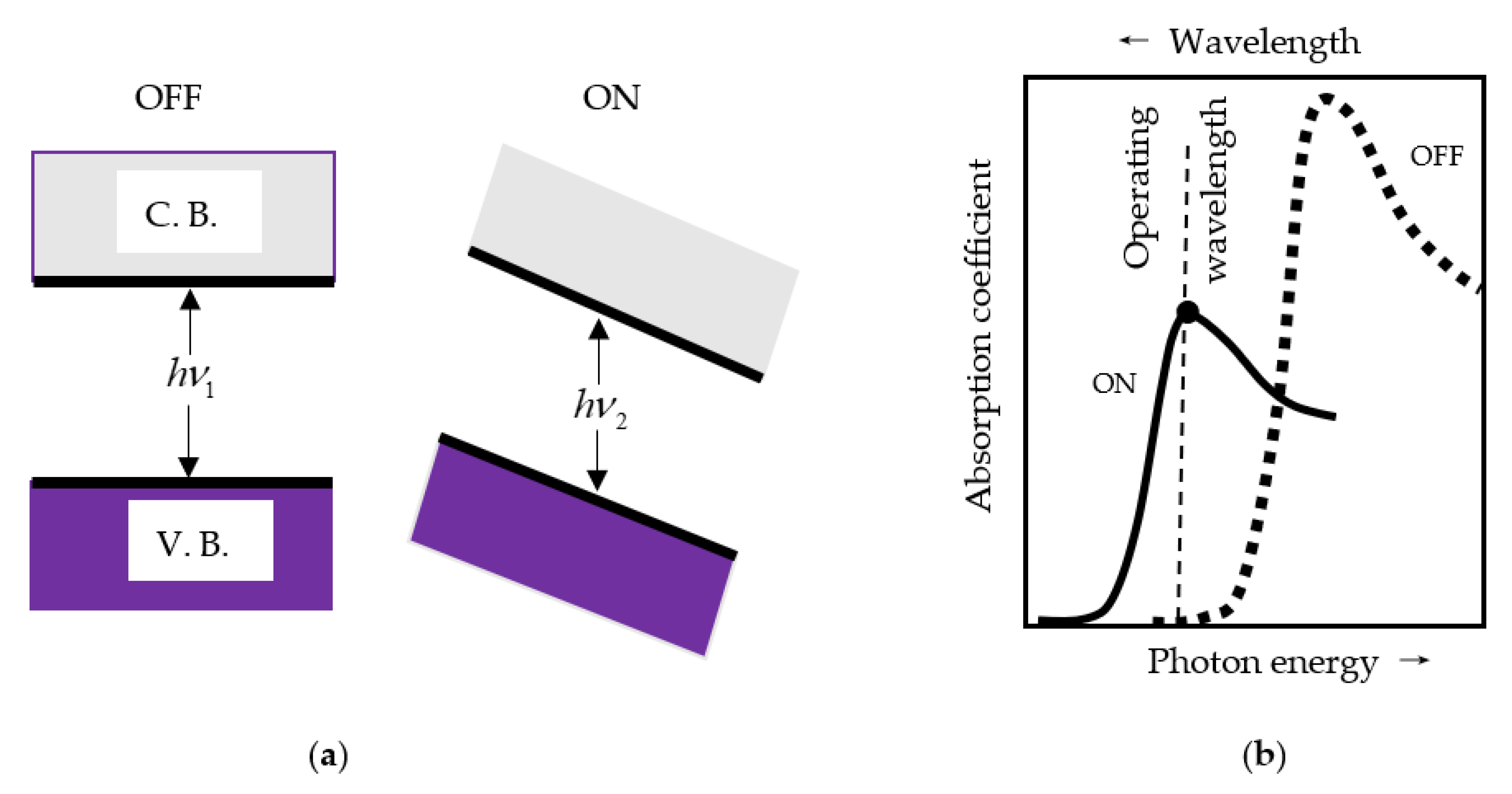
Electroabsorption is a change in the absorption characteristics of a material in response to an externally applied electric field [18]. The application of an external electric field leads to electron tunneling, which extends the absorption edge into the forbidden gap. The material bandgap energy is thus reduced below that provided by the band tail and Urbach tail. As shown in Figure 1a, we have , where and are the two bandgap energies corresponding to the two electric field states (OFF and ON, respectively). This is called the Franz–Keldysh effect, and it shifts the absorption spectrum to longer wavelength, as illustrated in Figure 1b. The applied electric field also results in the absorption broadening and the exciton absorption peak’s disappearance. This effect can be used in optical electroabsorption modulators. As shown in Figure 1b, an incident beam at the operating wavelength is transmitted without absorption when the electric field is off. However, the light is absorbed upon electric field application. In comparison with electro-optic modulators which operate based on the refractive-index response to an applied electric field, electroabsorption modulators typically operate at greater speeds and at lower voltages. The electroabsorption effect is more obvious in semiconductor multiquantum-well (MQW) structures [18]. When an electric field is applied in the confinement direction, an additional phenomenon occurs, called the quantum-confined Stark effect (QCSE). There are some merits of QCSE; for example, exciton ionization is inhibited and exciton energy levels remain unbroadened even at high field level. As a result of these MQW properties, the wavelength shift in the absorption peak is greater, and the edge is more abrupt than in bulk semiconductors. Other merits include higher speeds, larger extinction ratios, lower drive voltages and lower chirp. Chirp is defined as the ratio of the increments of the real and imaginary parts of an electroabsorption modulator’s complex refractive index, which is an important transmission characteristic.
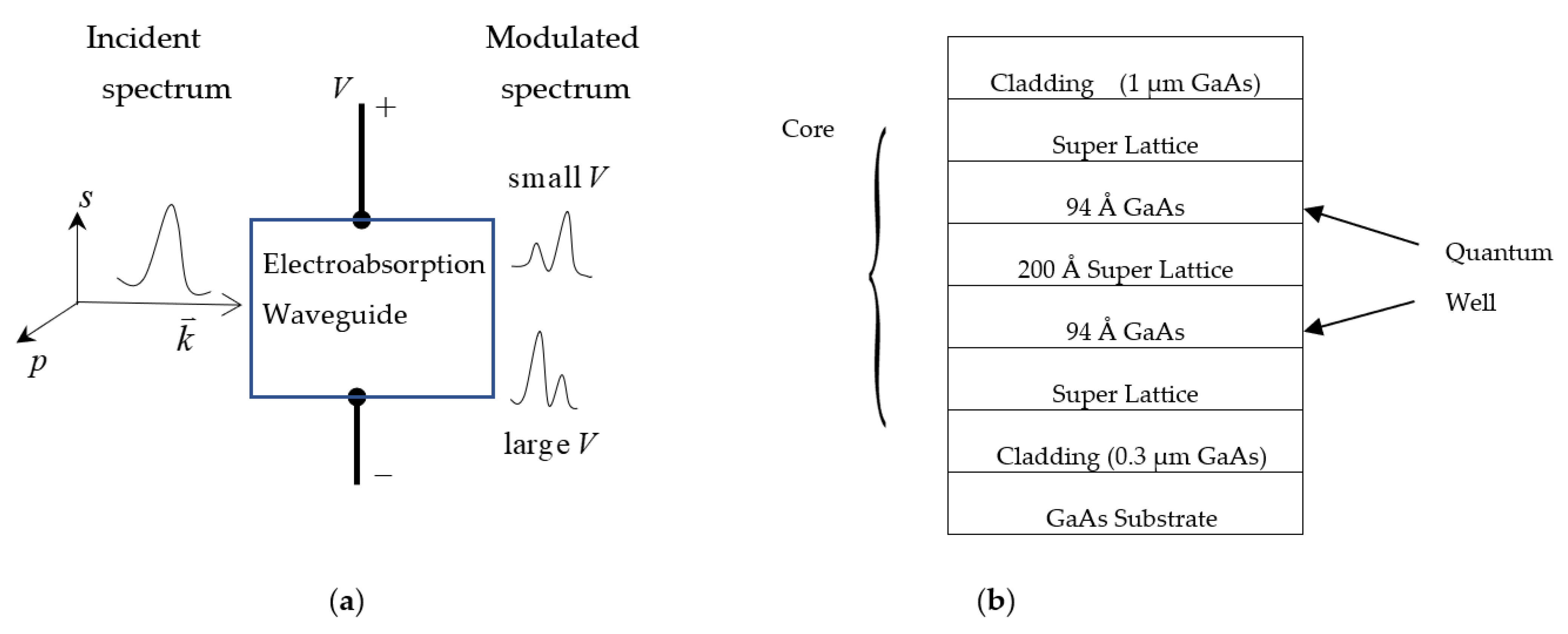
A GaAs/AlGaAs quantum-well waveguide [19,20] is used as an example. Its data transmission application configuration is illustrated in Figure 2a, and the electric field (denoted as voltage V in the figure) is perpendicularly applied to the layer plane. Note that the light travels along the plane of the layers (the wave vector in the figure, defined as ). Thus, light can propagate with its polarization either in the plane of the layers (p) or perpendicular to the plane (s), as indicated in Figure 2a. Additionally, the figure shows a spectral shift controlled by the magnitude of the applied voltage V, which will be explained in detail later. A Gaussian spectral beam is incident on the waveguide from the left. After traveling it and leaving from the right, the outgoing beam will have a different spectral shape depending on the voltage value, as plotted on the right side of the figure. A schematic structure of the waveguide is depicted in Figure 2b. The details can be found in [20]. Two 94 Å quantum wells were embedded in a 3.6 μm-thick superlattice which formed the waveguide core.
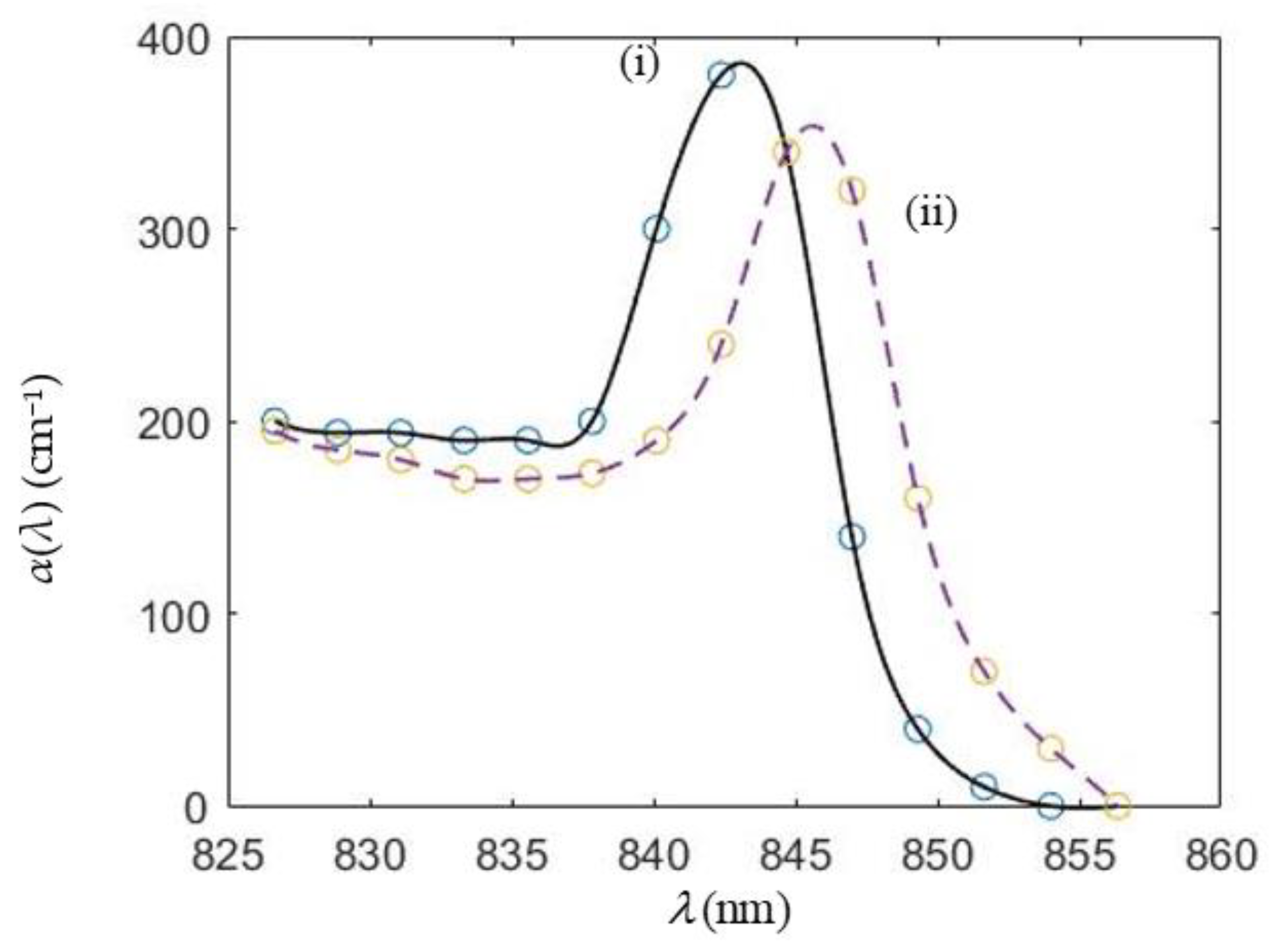
The sample was doped as a p–i–n diode, which was reverse biased to apply an electric field perpendicular to the quantum wells. It was designed so that a 150 μm-long sample would exhibit 10 dB modulation depth. The s-polarization mode is inaccessible to light propagating perpendicular to the layers and shows different selection rules [15]. Specifically, the heavy hole excitonic absorption effectively vanishes, and its strength is transferred into the single remaining light hole peak at higher photon energy. Figure 3 shows absorption spectra of the quantum-well waveguide for s-polarization mode as a function of the electric field applied perpendicular to the layers for (i) 1.6 × 10⁴ V/cm and (ii) 105 V/cm. The data marked with circles in the figure were adapted from Weiner [20] and are interpolated by cubic splines to give the curves. The light hole peaks are seen clearly and when the applied field is increased, the peak is decreased and broadened. Note that this method utilizes the waveguide mode to transmit the light signal, and the modes depend on the real part and imaginary part (related to the absorption) of the complex refractive index. Consequently, the change of the absorption spectra caused by the applied voltage may have some effects on the mode to different extents. However, because the length of the wave guide is short and the absorption spectra are not changed greatly (as seen in Figure 3), those effects may not be significant.
3. Results
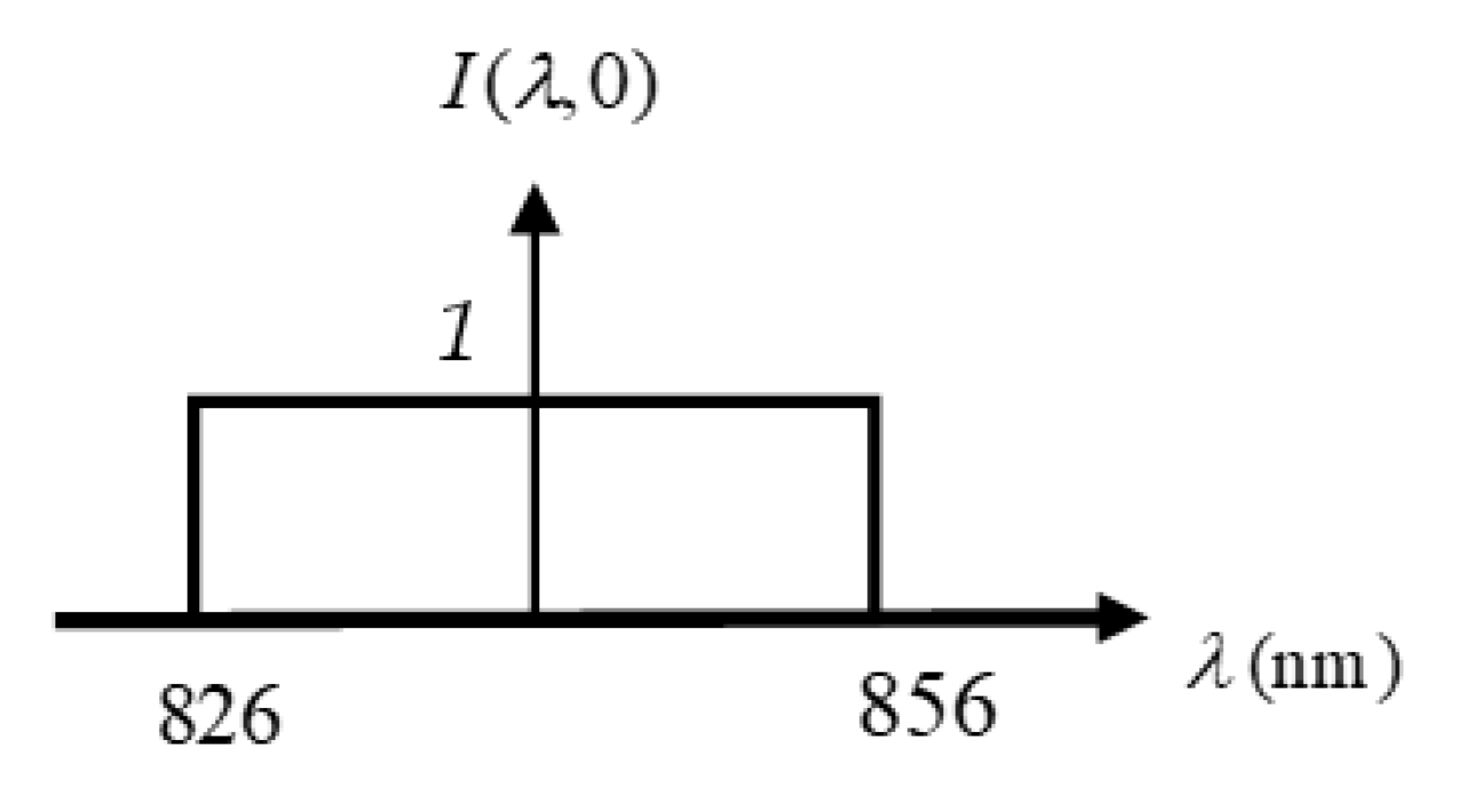
Now we can proceed to study the modulated light intensity under the applied electric field. First, we consider a uniform unit spectral intensity (spectrum) in the wavelength range from 826 nm to 856 nm, as shown in Figure 4. Beer’s law [21] is
where and are the incident intensity and the final one after propagating distance d, respectively, and is the absorption coefficient in Figure 3. Figure 5 shows the natural log of for d = 150 μm. The log function here makes the whole range of seen more clearly.
Now we turn our attention to how to use this effect to generate the spectral switch and use it to perform the data transmission task. Let us first use another type of spectrum, the normalized Gaussian one, in the form
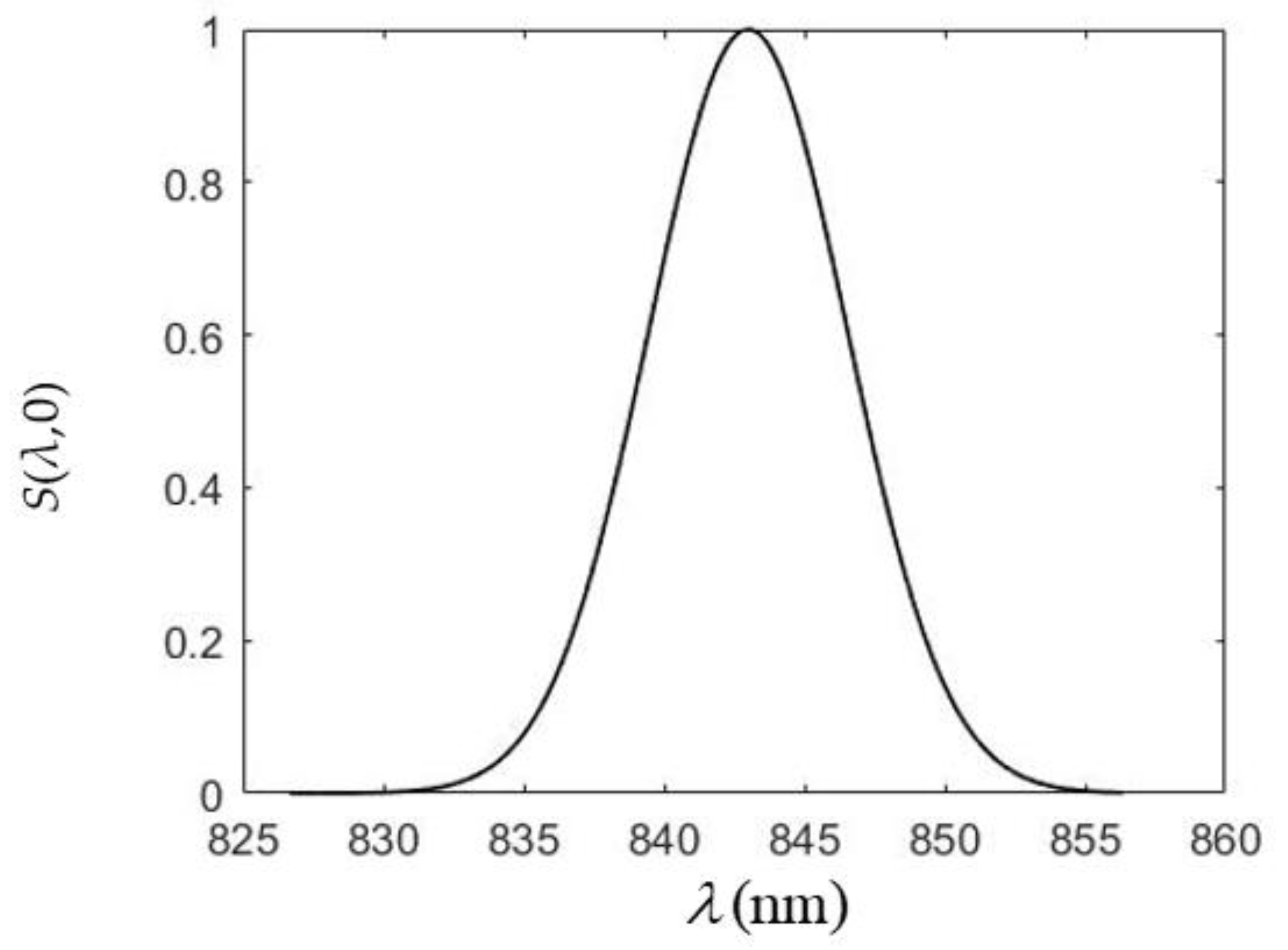
where and are the center wavelength and the spectral bandwidth, respectively. Here we use the symbol to differentiate from the used in Figure 4. It is plotted in Figure 6 for nm and nm.
When this Gaussian spectrum is incident to the same electroabsorption waveguide and travels the distance d, its spectral intensity again is where the normalized spectrum for the two different applied field values (see Figure 3) is plotted in Figure 7a,b, respectively. As seen in the figure, the spectral shift is a red shift (the peak moves to the right of the original incident peak) in Figure 7a, whereas it is a blue shift (the peak moves to the left of the original incident peak) in Figure 7b. Thus, the spectral shift can be controlled by the magnitude of the applied field. This behavior is called a spectral switch (SS); it appears in different schemes or occasions and has been studied in detail [7,22]. One of the SS applications is utilized in information encoding and transmission in free space [3,23]. Here, it can be used to transmit data in free space or on the chip scale because a waveguide device and light source of this sort can be fabricated and integrated on a single chip [18].
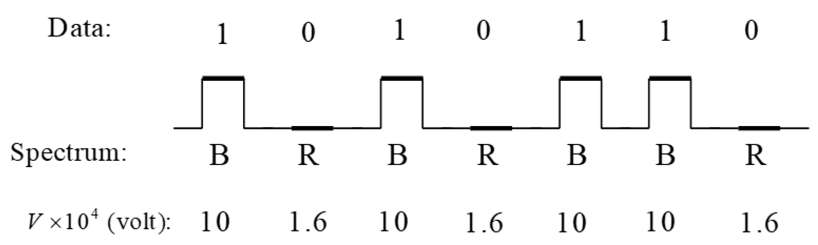
The scheme goes as follows. Consider a set of binary digital data (as shown in the first row of Figure 8) that needed to be transmitted through an electroabsorption device such as the one in Figure 2. Using the spectral shift manipulation by controlling the magnitude of the applied field as in Figure 3, we can designate blue shift and red shift as a bit of “1” or “0”, respectively. The notations B and R are used to indicate the blue shift and red shift in the third row of Figure 8, starting with the word “spectrum”. By properly adjusting the magnitude of the applied voltage (the bottom row of Figure 8) the blue shift or red shift in the spectrum peak can be controlled accordingly, as seen in Figure 7. The data can then be transmitted and detected or decoded by a receiver. Let us discuss the absolute efficiency of this method further. If we assume the incident Gaussian spectrum with 1.0 mW at the center wavelength nm, the absolute efficiency is 0.12 mW at nm for Figure 7a and the absolute efficiency is 0.042 mW at nm for Figure 7b. The output power magnitudes fall in the range from mW to µW, which can be easily detected by an available optical spectrum analyzer, such as an Anritsu MS9740B. The power is not too weak, for two reasons. First, the total length is only 150 μm. Second, the shifted spectrum peaks are not very near the center wavelength nm, which is at the dip of the first curve in Figure 5. Thus, the two shifted peak wavelengths can still have enough power to be detected.
As it is claimed as being a data transmission method, it is important to estimate the modulation speed. Basically, the achievable speed of our scheme depends on how fast a semiconductor multiquantum-well (MQW) electroabsorption structure can be modulated. Since the referenced work [20] does not give such information, we found another work with the same GaAs/AlGaAs quantum-well configuration studying this issue in detail [24]. The speed depends on the capacity and the load. As seen from Table 1 in [24], a resistive load with 47 kΩ has a 30 ns switching time and 28 ns RC time constant for a 100 μm-long sample, which is a good reference to our 150 μm-long sample [20]. The corresponding modulation speed is about 30 Mb/s, taking 30 ns switching time as the example. Afterwards, much higher speeds of 40 Gb/s were achieved by Cheng et al. [25].
4. Discussion and Conclusions
As mentioned in the Introduction, in the past a data-transmission scheme based on the EO effect to control the refractive index to manipulate the spectra was presented [3]. Here we use the electroabsorption effect to control the absorption coefficient and spectral shifts to perform the same task. The electroabsorption modulation typically operates at greater speeds and at lower voltages than electro-optic modulators, operating based on the refractive-index response to applied electric fields. The data can still be transmitted by modulating monochromatic light intensity. Nevertheless, one advantage of using polychromatic light spectral shift lies in that only the spectral shift (blue or red) needs to be judged or confirmed. This is independent of the absolute detected spectrum intensity. In the monochromatic light intensity modulation scheme, monitoring and maintaining correct intensities corresponding to bit 0 or 1 are necessary, and may be challenging. However, in the polychromatic scheme, an optical spectrum analyzer or fiber spectrometer is required to record the modulated spectrum.
It seems that this method is similar to the conventional frequency modulation (FM) because the shifted spectral peaks (red shift or blue shift) have different wavelengths (or frequencies). However, they are essentially different as explained below. Direct FM modulation can be achieved by directly feeding the message into the input of a voltage-controlled oscillator. Thus, at any instantaneous moment there is only one frequency component (a higher or lower one representing digital cone 1 or 0, respectively) being transmitted—it is a “frequency-changing” scheme. In our method, no oscillator is used, only an electroabsorption material is used to control the broad-band light source spectrum. There are many wavelength components that remain in the spectrum at any instantaneous moment, as can be seen in Figure 7. The digital data are encoded through the red/blue shift of the spectra; thus, it is a “spectral-shift” scheme.
This work studies in detail the effects of a semiconductor quantum-well waveguide’s electroabsorption on a polychromatic light. We demonstrated that for light sources with suitable central wavelength and bandwidth, the spectrum peak shifts can be controlled by varying the magnitude of the applied voltage. This feature can be employed to perform data transmission jobs on a chip scale, which is of value because the waveguide can be fabricated and integrated with a light source on a single chip. Possible candidates for this kind of polychromatic light source include LEDs or edge emitting light emitting diodes (ELEDs). Compared with its monochromatic counterpart, such as DFB lasers, LEDs (or ELEDs) have the advantages of simple structure, easy fabrication and low cost.
Author Contributions
Conceptualization, P.H.; methodology, J.-P.C.; validation, J.-H.W.; data curation, H.-C.H.; writing—original draft preparation, H.-C.H.; writing—review and editing, P.-Y.L.; writing—review and editing, P.H.; funding acquisition, P.H. All authors have read and agreed to the published version of the manuscript.
Funding
This work was supported by the Ministry of Science and Technology (MOST) of Taiwan under contract number MOST 107-2221-E-005-059-MY3.
Institutional Review Board Statement
Not applicable.
Informed Consent Statement
Not applicable.
Acknowledgments
We would like to express our thanks for the support from National Chung Hsing University, and Central Taiwan Science Park 110RB02.
Conflicts of Interest
The authors declare no conflict of interest.
References
- Wolf, E. Invariance of the spectrum of light on propagation. Phys. Rev. Lett. 1986, 56, 1370–1372. [Google Scholar] [CrossRef] [PubMed]
- Wolf, E. Red shifts and blue shifts of spectral lines emitted by two correlated sources. Phys. Rev. Lett. 1987, 58, 2646–2648. [Google Scholar] [CrossRef] [PubMed]
- Han, P. Electro-optic modulation for spectral switches and phase singularities of a double slit in the far field. J. Opt. 2011, 13, 035713. [Google Scholar] [CrossRef]
- Hsu, H.C.; Han, P. Spectra manipulation with the photorefractive effect via the spatial–spectral correspondence relationship. J. Opt. Soc. Am. A 2020, 37, 219–224. [Google Scholar] [CrossRef] [PubMed]
- Wolf, E. Non-cosmological redshifts of spectral lines. Nature 1987, 326, 363–365. [Google Scholar] [CrossRef]
- Ding, C.L.; Pan, L.Z.; Lü, B. Changes in the spectrum, polarization, and coherence of stochastic spatially and spectrally partially coherent electromagnetic J0-correlated Schell-model pulsed beams propagating in free space. Eur. Phys. J. D 2010, 59, 329–336. [Google Scholar] [CrossRef]
- Pu, J.; Zhang, H.; Nemoto, S. Spectral shifts and spectral switches of partially coherent light passing through an aperture. Opt. Commun. 1999, 162, 57–63. [Google Scholar] [CrossRef]
- Han, P. Lattice spectroscopy. Opt. Lett. 2009, 34, 1303–1305. [Google Scholar] [CrossRef] [PubMed]
- Visser, T.D.; Wolf, E. Spectral anomalies near phase singularities in partially coherent focused wavefields. J. Opt. A Pure Appl. Opt. 2003, 5, 371–373. [Google Scholar] [CrossRef]
- Rasouli, S.; Khazaei, A.M.; Hebri, D. Talbot carpet at the transverseplane produced in the diffraction of plane wave from amplituderadial gratings. J. Opt. Soc. Am. A 2018, 35, 55–64. [Google Scholar] [CrossRef] [PubMed]
- Kanseri, B.; Gyaprasad; Rathi, A.K. Broadband spectral shaping using nematic liquid crystal. Results Phys. 2019, 12, 531–534. [Google Scholar] [CrossRef]
- Friberg, A.T.; Wolf, E. Relationships between the complex degrees of coherence in the space-time and in the space-frequency domains. Opt. Lett. 1995, 20, 623–625. [Google Scholar] [CrossRef] [PubMed]
- Joshi, S.; Yadav, B.K.; Verma, M.; Khan, M.S.; Kandpal, H.C. Effect of polarization on spectral anomalies of diffracted stochastic electromagnetic beams. J. Opt. 2013, 15, 035405. [Google Scholar] [CrossRef]
- Verma, M.; Joshi, S.; Bisht, N.; Kandpal, H.C.; Senthilkumaran, P.; Joseph, J. Effect of surface plasmons on spectral switching of polychromatic light with Au-double-slit. J. Opt. Soc. Am. A 2012, 29, 195–199. [Google Scholar] [CrossRef] [PubMed]
- Soskin, M.S.; Vasnetov, M.V. Singular optics. In Progress in Optics; Wolf, E., Ed.; Elsevier: Amsterdam, The Netherlands, 2001; Volume 42, pp. 219–276. [Google Scholar]
- Mark, R.D.; Kevin, O.; Miles, J.P. Singular optics: Optical Vortices and Polarization Singularities. In Progress in Optics; Wolf, E., Ed.; Elsevier: Amsterdam, The Netherlands, 2009; Volume 53, pp. 293–363. [Google Scholar]
- Han, P. Spatial–Spectral Correspondence Relationship for Mono—Poly chromatic Light Diffraction. In Progress in Optics; Visser, T.D., Ed.; Elsevier: Amsterdam, The Netherlands, 2018; Volume 63, pp. 33–87. [Google Scholar]
- Saleh, B.E.A.; Teich, M.C. Fundamentals of Photonics, 2nd ed.; John Wiley & Sons: New York, NY, USA, 2007; p. 868. [Google Scholar]
- Islam, M.N.; Hillman, R.L.; Miller, D.A.B.; Chemla, D.S. Electroabsorption in GaAs/AlGaAs coupled quantum well waveguides. Appl. Phys. Lett. 1987, 50, 1098–1100. [Google Scholar] [CrossRef]
- Weiner, J.S.; Miller, D.A.B.; Chemla, D.S.; Damen, T.C. Strong polarization-sensitive electroabsorption in GaAs/AlGaAs quantum well waveguide. Appl. Phys. Lett. 1985, 47, 1148–1150. [Google Scholar] [CrossRef]
- Born, M.; Wolf, E. Principles of Optics, 7th ed.; Cambridge University Press: Cambridge, UK, 1999; p. 219. [Google Scholar]
- Pu, J.; Nemoto, S. Spectral shifts and spectral switches in diffraction of partially coherent light by a circular aperture. IEEE J. Quantum Electron. 2000, 36, 1407–1411. [Google Scholar]
- Pu, J.; Cai, C. Spectral anomalies in Young’s double-slit interference experiment. Opt. Express 2004, 12, 5131–5139. [Google Scholar] [CrossRef] [PubMed]
- Miller, D.; Chemla, D.; Damen, T.; Wood, T.; Burrus, C.; Gossard, A.; Wiegmann, W. The Quantum Well Self-Electrooptic Effect Device: Optoelectronic Bistability and Oscillation, and Self-Linearized Modulation. IEEE J. Quantum Electron. 1985, QE-21, 1462–1476. [Google Scholar] [CrossRef]
- Cheng, Y.; Pan, J.; Wang, Y.; Zhou, F.; Wang, B.; Zhao, L.; Zhu, H.; Wang, W. 40-Gb/s Low Chirp Electroabsorption Modulator Integrated With DFB Laser. IEEE Photonics Technol. Lett. 2009, 21, 356–359. [Google Scholar] [CrossRef]
Figure 1.
The Franz–Keldysh effect. (a) The bandgap in the absence of an external electric field (OFF) is reduced in its presence (ON). (b) Change in the absorption spectrum caused by the presence of an electric field. The absorption peak moves toward longer wavelengths. C. B. and V. B are conduction band and valence band, respectively.

Figure 2.
(a) The waveguide device configuration used in spectrum peak shift control. (b) The waveguide schematic structure.
Figure 2.
(a) The waveguide device configuration used in spectrum peak shift control. (b) The waveguide schematic structure.

Figure 3.
The absorption spectra of the quantum well waveguide for the s-polarization mode as a function of the electric field applied perpendicular to the layers. (i) 1.6 × 10⁴ V/cm and (ii) 105 V/cm [20]. The solid line and dashed line correspond to the two applied voltage values respectively. The circle markers on the lines are used for cubic spline interpolation.

Figure 4.
The spectral distribution of a unit uniform spectrum.

Figure 5.
The natural log of for d = 150 μm corresponding to the two curves in Figure 3. (i) 1.6 × 10⁴ V/cm and (ii) 105 V/cm.
Figure 5.
The natural log of for d = 150 μm corresponding to the two curves in Figure 3. (i) 1.6 × 10⁴ V/cm and (ii) 105 V/cm.

Figure 6.
The spectral distribution of a Gaussian spectrum.

Figure 7.
The normalized spectral distribution of a unit Gaussian spectrum in Figure 6. (a) Red shift for V = 1.6 × 10⁴ V/cm. (b) Blue shift for V = 105 V/cm. (i) 1.6 × 10⁴ V/cm and (ii) 105 V/cm.
Figure 7.
The normalized spectral distribution of a unit Gaussian spectrum in Figure 6. (a) Red shift for V = 1.6 × 10⁴ V/cm. (b) Blue shift for V = 105 V/cm. (i) 1.6 × 10⁴ V/cm and (ii) 105 V/cm.

Figure 8.
Illustration for the data encoding and transmission by controlling the magnitude of the applied field. The two-level data 0 and 1 are related to the spectral shifts R and B, respectively, which can be obtained by varying the magnitude of the applied voltage V.
Figure 8.
Illustration for the data encoding and transmission by controlling the magnitude of the applied field. The two-level data 0 and 1 are related to the spectral shifts R and B, respectively, which can be obtained by varying the magnitude of the applied voltage V.

Publisher’s Note: MDPI stays neutral with regard to jurisdictional claims in published maps and institutional affiliations. |
© 2022 by the authors. Licensee MDPI, Basel, Switzerland. This article is an open access article distributed under the terms and conditions of the Creative Commons Attribution (CC BY) license (https://creativecommons.org/licenses/by/4.0/).
Share and Cite
MDPI and ACS Style
Chang, J.-P.; Weng, J.-H.; Hsu, H.-C.; Lee, P.-Y.; Han, P. A Data Transmission Method with Spectral Switches via Electroabsorption. Appl. Sci. 2022, 12, 979. https://0-doi-org.brum.beds.ac.uk/10.3390/app12030979
AMA Style
Chang J-P, Weng J-H, Hsu H-C, Lee P-Y, Han P. A Data Transmission Method with Spectral Switches via Electroabsorption. Applied Sciences. 2022; 12(3):979. https://0-doi-org.brum.beds.ac.uk/10.3390/app12030979
Chicago/Turabian StyleChang, Jyun-Ping, Jun-Hong Weng, Hsun-Ching Hsu, Pei-Yuan Lee, and Pin Han. 2022. "A Data Transmission Method with Spectral Switches via Electroabsorption" Applied Sciences 12, no. 3: 979. https://0-doi-org.brum.beds.ac.uk/10.3390/app12030979
Note that from the first issue of 2016, this journal uses article numbers instead of page numbers. See further details here.