1. Introduction
Space mission requirements are critical and normally constitute a significant challenge for the development of a specific payload and the selection of the most suitable technology solution. In addition to performance requirements, payload design must also address limited spacecraft resources, such as power and total mass. In this context, the design of a space instrument, such as a LiDAR (Light Detection and Ranging) [
1,
2,
3,
4,
5], entails specific experimental research.
A LiDAR is a laser-based instrument that uses the time-of-flight technique [
6]. The emitted laser pulse travels from the instrument to a given object surface, and the scattered photons are subsequently received by the instrument’s detector. The distance from the instrument to the object can then be simply determined by comparing the time between the emission of the laser pulse and the detection. LiDAR may be applied to landing missions, spacecraft autonomous navigation near asteroids, to avoid collisions, or to assist operations [
7,
8].
The overall efficiency of this equipment in view of space applications should then be improved in order to reduce the size, weight, and power (SWaP) factor. Highly efficient laser pulsed sources associated with reduced noise and a high-gain receiver are obvious key factors in this quest.
Microchip lasers can be used as the laser source of a LiDAR [
9]. These are solid-state lasers with optical cavities in the range of millimeters that may achieve pulsed operation with 50 kW peak power and 100 µJ pulse energy at low power consumption [
10], an attractive solution with low impact on spacecraft resources. Laser diode-pumped configurations for passively Q-switched microchip lasers have already been published and serve as a basis for this study [
10,
11,
12].
Regarding the receiver section of the LiDAR and the detection of the backscattered pulse, the capability of single photon detection has been an important development driver [
13,
14], mostly in terms of the power budget for maximized range operation.
This paper presents the results of an investigation into cavity assembly techniques for the construction of a pulsed microchip laser. This consisted of an Yb-Er: glass active medium passively Q-switched by a Co:MgAl
2O
4 saturable absorber. Results from the research on the performance of detection instrumentation in a space representative environment are also addressed. An avalanche photodiode (APD) along with the respective transimpedance amplifier (TIA) was tested at low temperatures and under vacuum using a custom-built chamber. Results are also presented for a simple passive quenching circuit (PQC) [
15] with high polarization voltages applied to the detection system but at normal pressure and temperature.
The solutions studied for the two key components presented in this work can support the development of an overall LiDAR architecture based on a miniaturized high peak power microchip laser associated with a receiver solution based on a high sustained gain avalanche sensor.
This paper has the following structure:
Section 2 presents the breadboard design and implementation of the microchip laser;
Section 3 presents the APD breadboard designs and implementations; and
Section 4 outlines the conclusions.
2. Microchip Laser
The microchip laser is a solid-state laser that is efficient and compact, which makes it very practical for space applications. The components of the laser have small dimensions, which results in a short optical cavity in the range of millimeters. They can be optically pumped using a laser diode, and there are already configurations for passively Q-switched microchip lasers [
16,
17,
18,
19,
20,
21].
In this work, a manufacturing assembly process was developed and tested to produce a microchip laser cavity with pulsed emission. An erbium glass as the active medium, a Co:Spinel glass as a Q-switch, and an external output coupler were used for the purpose. For safety reasons, the wavelength of the emission of the LiDAR should operate in the “eye-safe” region of the spectrum. The erbium ions emit in the 1550 nm wavelength region, which is considered “eye-safe”.
The microchip laser was implemented in two setups. In the first, the glass components of the laser were placed in special holders that allowed movement between them. Their alignment forms the microchip’s optical cavity. In the second setup, the glass components were glued to a common substrate. The pumping of the microchip laser was performed by a laser diode coupled with an optical fiber. The light emitted was collimated and focused with a lens with a focal length of 35 mm. The pump laser had a typical wavelength of 975 nm, which corresponds to an absorption peak of the active medium material. Pumping was performed with quasi-continuous wave (QCW) emission to prevent damage to the active medium and its coatings. Its frequency was 10 Hz, with 10 ms of pulse width and 100 ms of pulse period.
2.1. Design of Movable Cavities
The first setup is based on previous works [
22,
23,
24]. It allowed comparisons between different configurations of laser cavities. For this, four optical components were used. The active medium (AM) was an erbium and ytterbium co-doped phosphate glass with either 1 mm or 1.5 mm of thickness. Both glasses had the same doping concentrations,
with a concentration of
and
with
, and highly reflective (HR) at 1550 nm (HR@1550 nm) coatings as input couplers. The output coupler (OC) was a silica glass with a HR@1550 nm coating with 98% reflectivity. The Q-switch was a saturable absorber (SA) of Co:Spinel glass with an initial transmission of 98%.
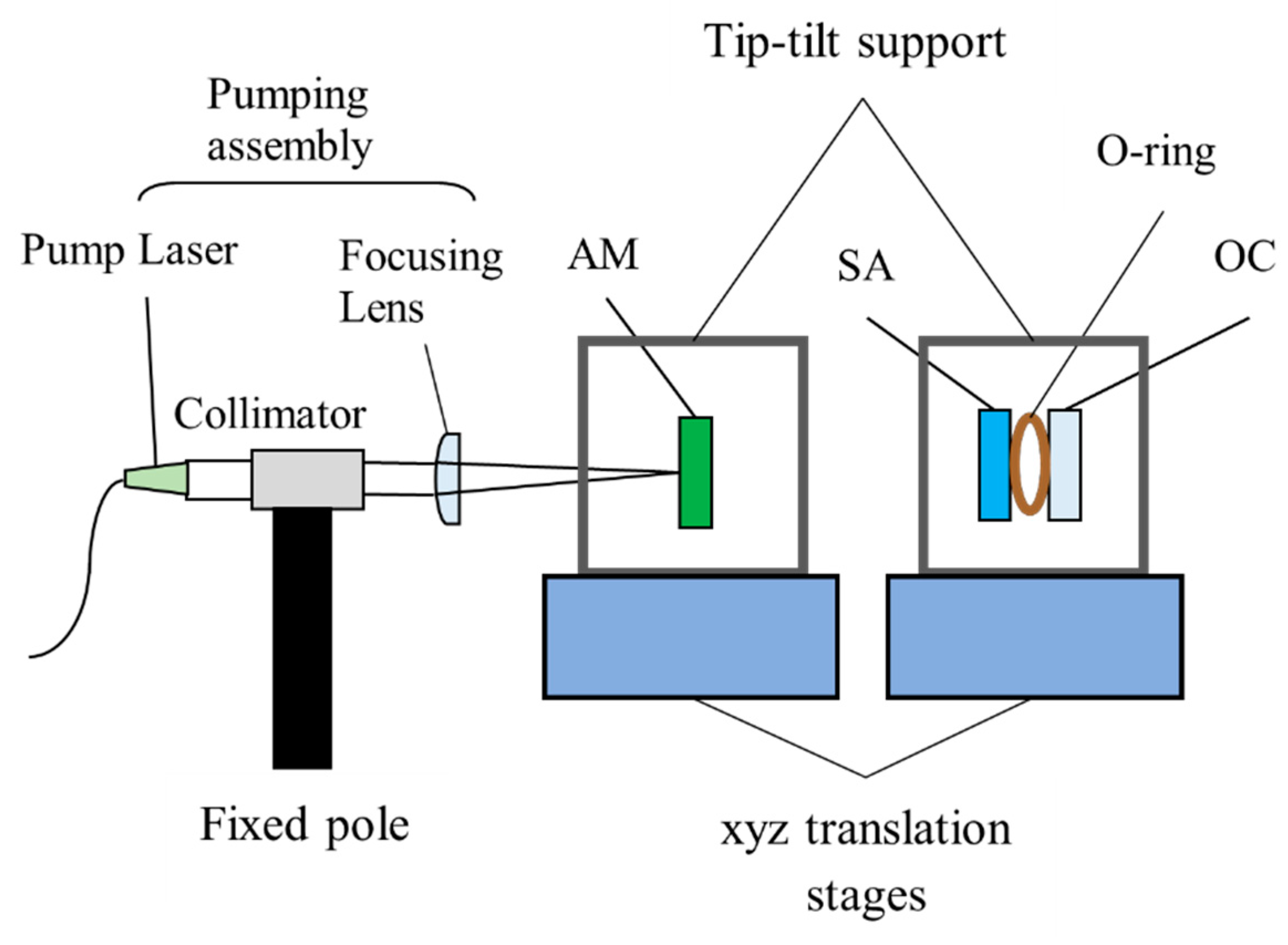
To allow the alignment of the glass components in the assembly, aluminum holders were designed and manufactured to fit the equipment. This allowed small changes in the XYZ axes and tip-tilt movements. Setup for the assembly of the microchip laser during the first implementation is shown in
Figure 1.
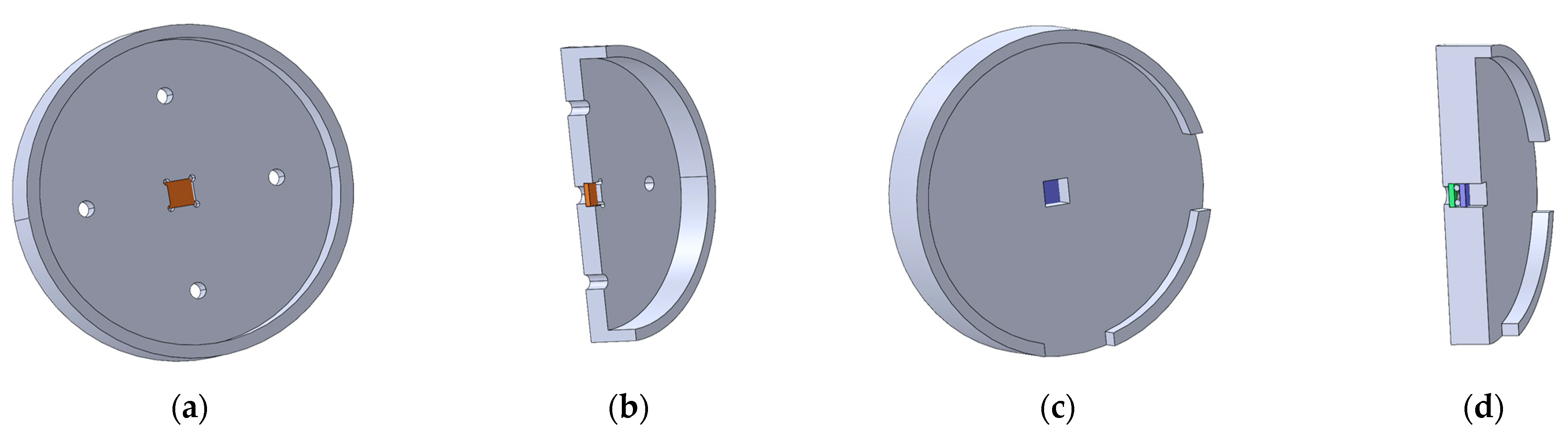
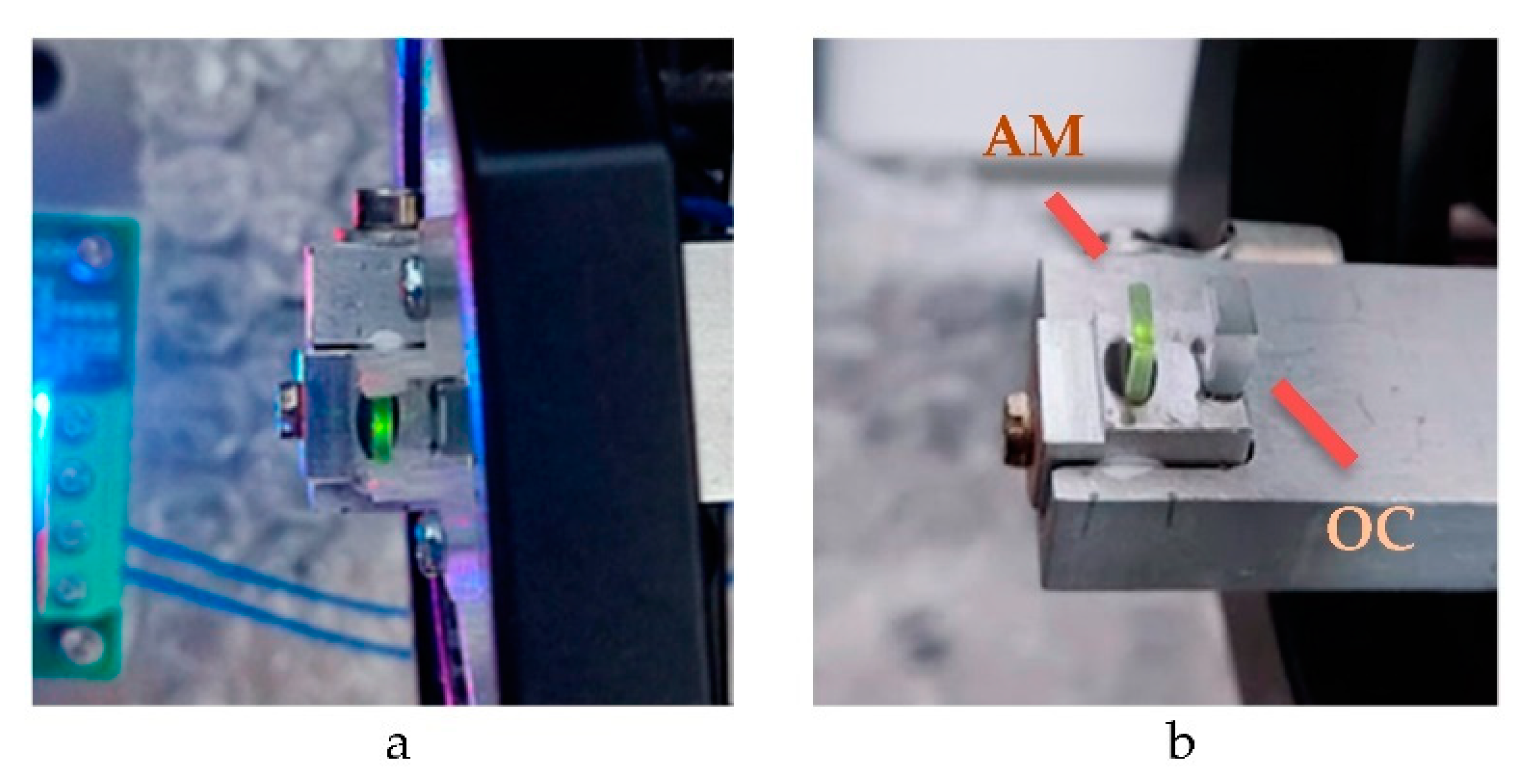
The active medium crystal was mounted on an aluminum holder, as shown in
Figure 2a,b. The output coupler and the Q-switch were placed in another aluminum holder designed and manufactured to hold both. They were separated by a Viton O-ring, as shown in
Figure 2c,d. The computer-aided design (CAD) of the aluminum holder allowed the alignment of both glasses with the assembly axis as well as the alignment between the two.
Each optical glass was assembled and aligned individually. The alignment used a visible-spectrum (600 nm) laser and the specular back reflections of the individual items. After the first alignment of the output coupler and Q-switch using the alignment laser, an active alignment process was performed. The active alignment was carried out with the pump laser on and by adjusting the angles (tips/tilts) of the active medium and output coupler. The first detection of emission was made with the support of an infrared detector card in front of the laser cavity. With the microchip laser cavity aligned, the emission was characterized by a measure of the output optical power for each pumping level, the pulse shape, and the emission spectrum.
2.2. Design of Fixed Cavity
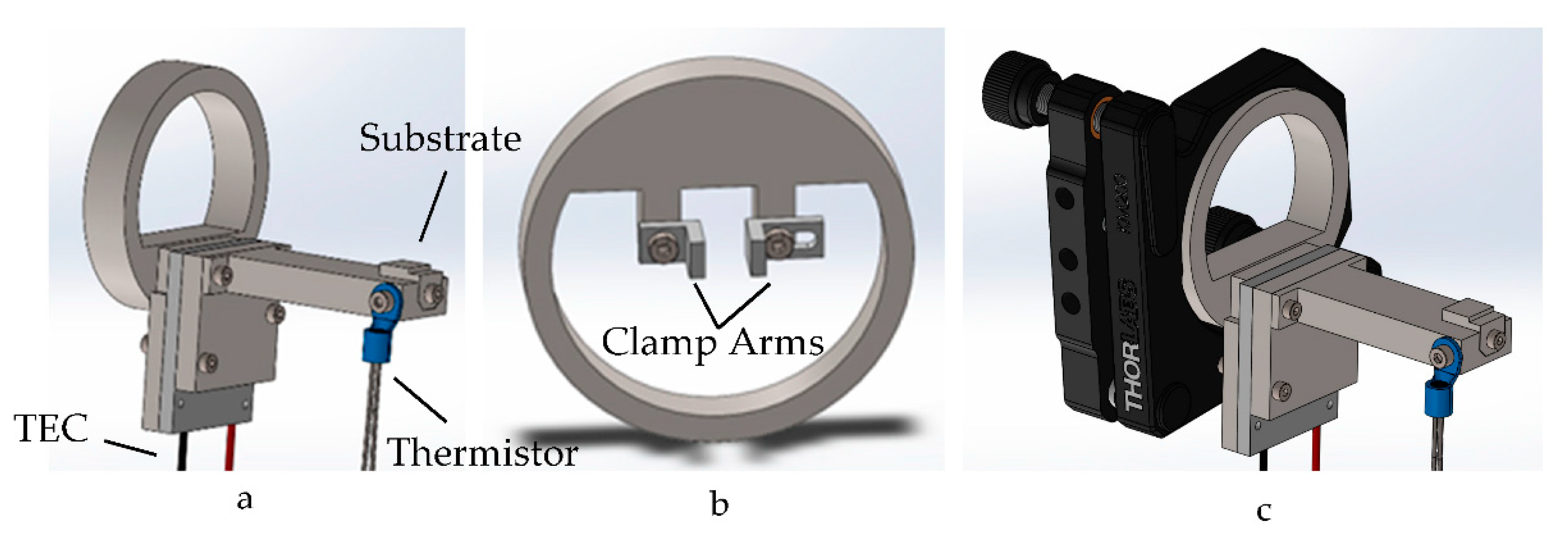
In the second setup, the optomechanics used for mounting and positioning the laser cavity components were reviewed. As such, the assembly of the fixed optical cavity used a setup similar to the one shown in
Figure 1. To hold the glass components, aluminum and Polyethylene Terephthalate Glycol (PETG) material (3D printed parts) clamps were designed and manufactured. The set of new aluminum and 3D printed parts (shown in
Figure 3) substituted the previous aluminum holders (shown in
Figure 1). The gluing of the optical components to a common substrate allowed for easier integration with the pumping system of the microchip laser. The active medium used had a thickness of 1 mm. An assembly table was designed for this purpose, and a procedure was drawn. The resulting cavity was characterized.
The glue used to secure the glass components to the aluminum substrate needed to be heated to 66 °C. For this reason, a system to hold and heat up the aluminum substrate was designed and manufactured, as shown in
Figure 3. In
Figure 3a, the heating system for the substrate is presented, and in
Figure 3b, the clamp for the glass components is detailed. The heating system for the substrate assembled in the optomechanics is shown in
Figure 3c.
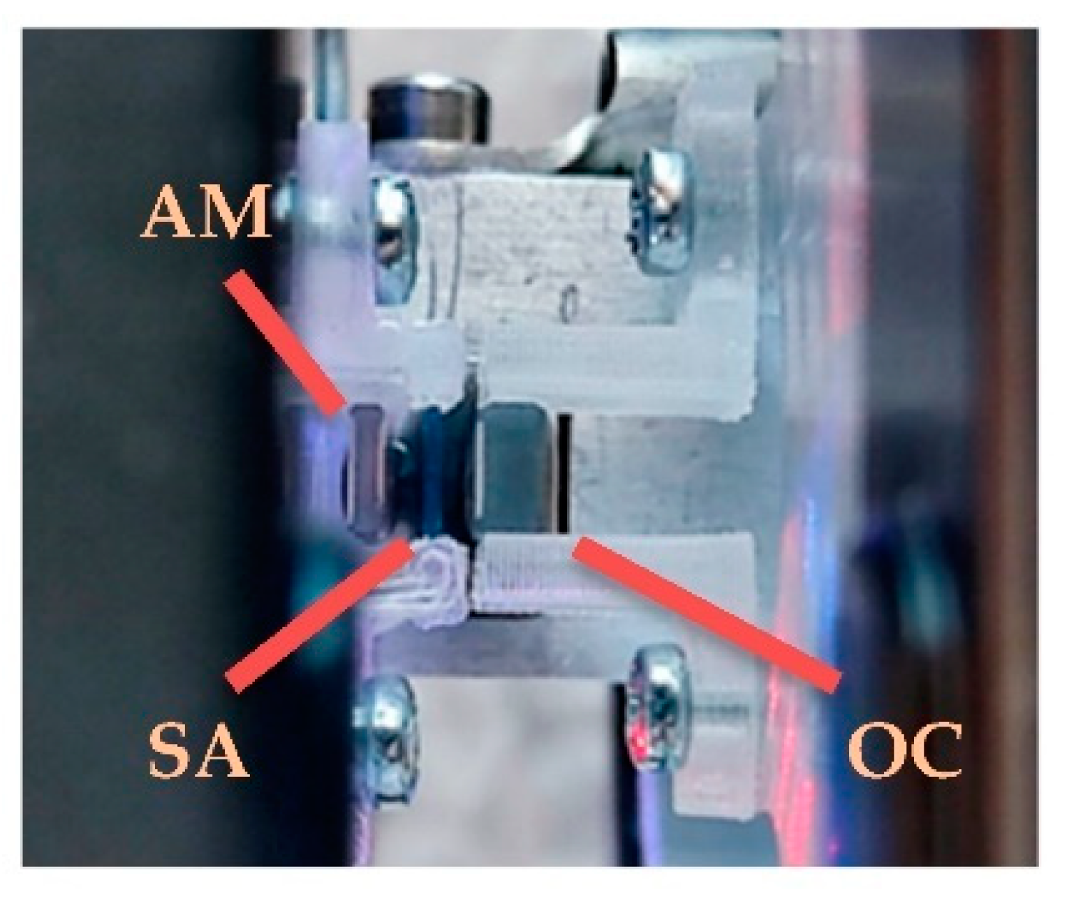
Three attempts at the gluing of the cavity were necessary to reach success, the main limitation being the shrinkage of the glue during the curing process. The first attempt consisted of the gluing of the active medium, followed by the gluing of both the output coupler and Q-switch simultaneously. The second gluing is shown in
Figure 4.
The first attempt was not successful because the laser emission disappeared during the second gluing. The output coupler and Q-switch were removed from the substrate for a second attempt. For the second attempt, the procedure was modified to separate the gluing of the Q-switch and the output coupler. Instead of being conducted simultaneously, the output coupler was glued first, followed by the gluing of the Q-switch. During the gluing of the Q-switch, the emission disappeared, and the process was stopped. During the removal of the Q-switch from the substrate, the active medium came loose.
For the third attempt, the active medium was glued first. This process is shown in
Figure 5a. After the gluing of the active medium, laser emission was observed. Without gluing the Q-switch, the emission obtained from this cavity was not stable. After several attempts at aligning the Q-switch to obtain pulsed laser emission, the third attempt was considered successful in assembling a fixed optical cavity with continuous wave (CW) emission, shown in
Figure 5b.
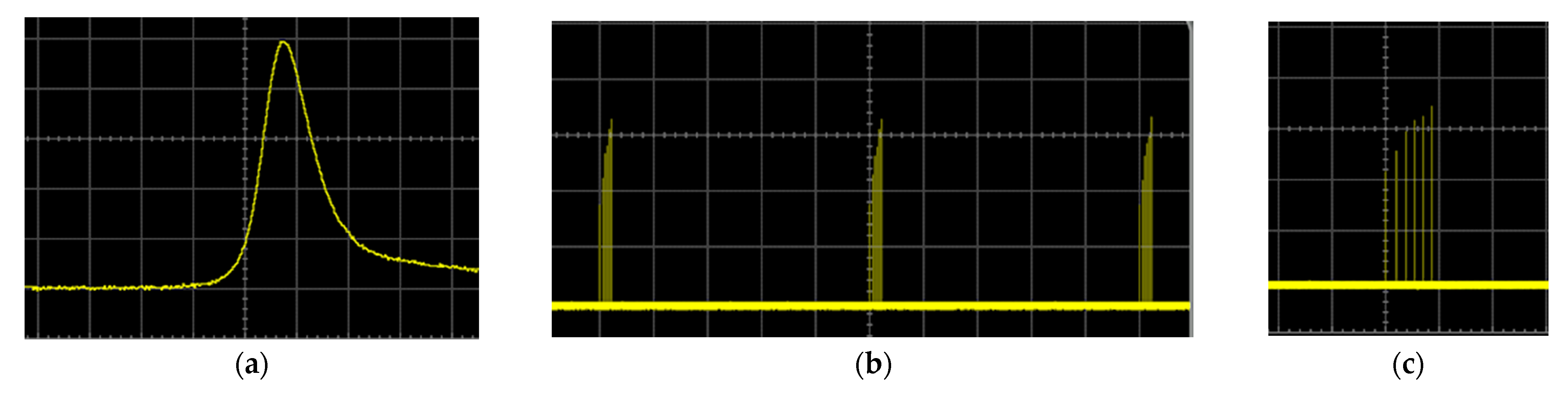
The pulse shape for each cavity emission was observed (see
Figure 6), and the energy and peak power of the pulses are presented in
Section 2.3. The dependency of the output optical power with the pumping power was measured (see
Figure 7).
2.3. Breadboard Results
The results from the characterization of the optical cavities of the microchip laser are presented in
Table 1.
Table 1 is divided into four columns for each configuration (Conf. 1 to Conf. 4). Conf. 1 has an active medium with 1 mm of thickness and no Q-switch. Conf. 2 has an active medium 1.5 mm thick and no Q-switch. Since there is no Q-switching element inside the cavities, Conf. 1 and Conf. 2 have CW emission. Conf. 3 has an active medium 1 mm thick and a Q-switch inside the cavity. Conf. 4 has an active medium with 1.5 mm of thickness and a Q-switch as well. The addition of the Q-switch inside the cavities allows Conf. 3 and Conf. 4 to have pulse laser emissions.
The cavity configuration chosen for the second setup of the microchip laser was Conf. 3, so the results will be focused on this one. The first step in the configuration of this cavity was determining the curve of the average output optical power versus the average optical pumping power. The slope efficiency of the laser was calculated to be around 8.5%. The shape of the pulse observed on the oscilloscope is shown in
Figure 6, with the time division being in
Figure 6a (10 ns), in
Figure 6b (20 ms), and
Figure 6c (5 ms).
Figure 6a shows a single micro-pulse observed on the oscilloscope from the first setup of the microchip laser;
Figure 6b is the burst emission, demonstrated in a viewing of three bursts; and
Figure 6c is a single burst. The energy and peak power values taken from the first implementation of the microchip laser are presented in
Table 2.
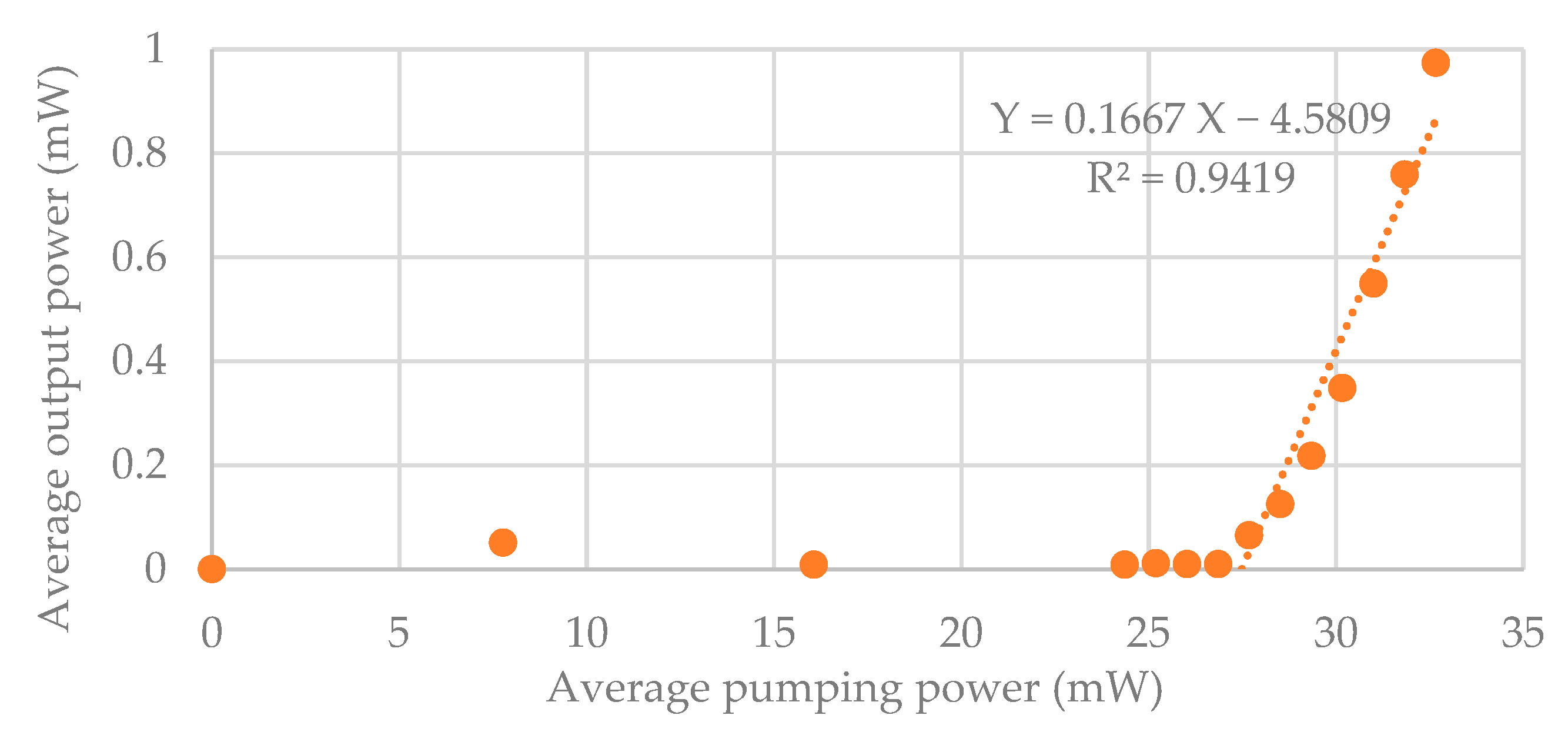
From the emission spectrum, it was possible to conclude that the microchip laser presents a wavelength value around 1532 nm. The optical path calculations for the cavity length result in 6 ± 1 mm. The resulting CW fixed optical cavity from the second setup was characterized by the curve of the average output optical power versus the average input optical power, shown in
Figure 7.
In
Figure 7, there is a slope efficiency value of around 16.7% (taken from the linear regression slope). It is a slight increase from the Conf. 1 cavity assembled in the first implementation, which had a slope efficiency of 16.0%.
2.4. Discussion
The laser emissions from the microchip laser cavities presented different efficiencies according to their configurations. It is observed that the additional thickness of the active medium in this case and/or the addition of the saturable absorber reduce the efficiency of the laser, as seen in
Table 1. The resulting fixed optical cavity presented a better efficiency (16.7%) than the movable cavity with the same configuration (16.0%). This is likely due to the shorter cavity assembled on the substrate.
3. APD Breadboard Design and Implementation
In this section, we report the development of the APD breadboard. The objective was to develop a sensor breadboard setup that allowed the testing of a highly sensitive sensor for LiDAR applications.
In a time-of-flight (TOF) LiDAR, a light pulse is emitted and a fraction of it is detected, then a timing trigger is given to the electronics to start the time counting. The light travels and is backscattered on a target surface. For long distances, a very small fraction of light is received by the LiDAR receiver aperture, and time counting is stopped. In this way, it is possible to compute a distance. The capacity to detect lower-power light pulses enables LiDAR operation at longer distances [
6,
13,
14].
The sensor used in the tests, Hamamatsu G14858-0020AB, is a high-speed and high-gain Indium Gallium Arsenide (InGaAs) semiconductor APD with an active area of 200 µm in diameter, working in the near infrared region. To detect the optical signals, the avalanche sensor must be operated in a reverse bias condition [
25,
26]. Usually, InGaAs sensors have usable gains ranging from 10 to 40. According to the manufacturer’s datasheet, the considered APD has gains up to 40, and its performance is characterized by gain = 10. In this work, we have tested the APD to very high gains of around ~261. This was achieved by implementing quenching circuitry and decreasing the operation temperature of the APD.
To characterize the performance of the sensor in the avalanche zone and near Geiger mode regions, the APD was tested at a wide temperature range and excited with different optical powers. This was carried out with the support of a small, custom-made vacuum chamber and a cascade-performance thermoelectric cooler (TEC) system.
3.1. Sensor Test Chamber
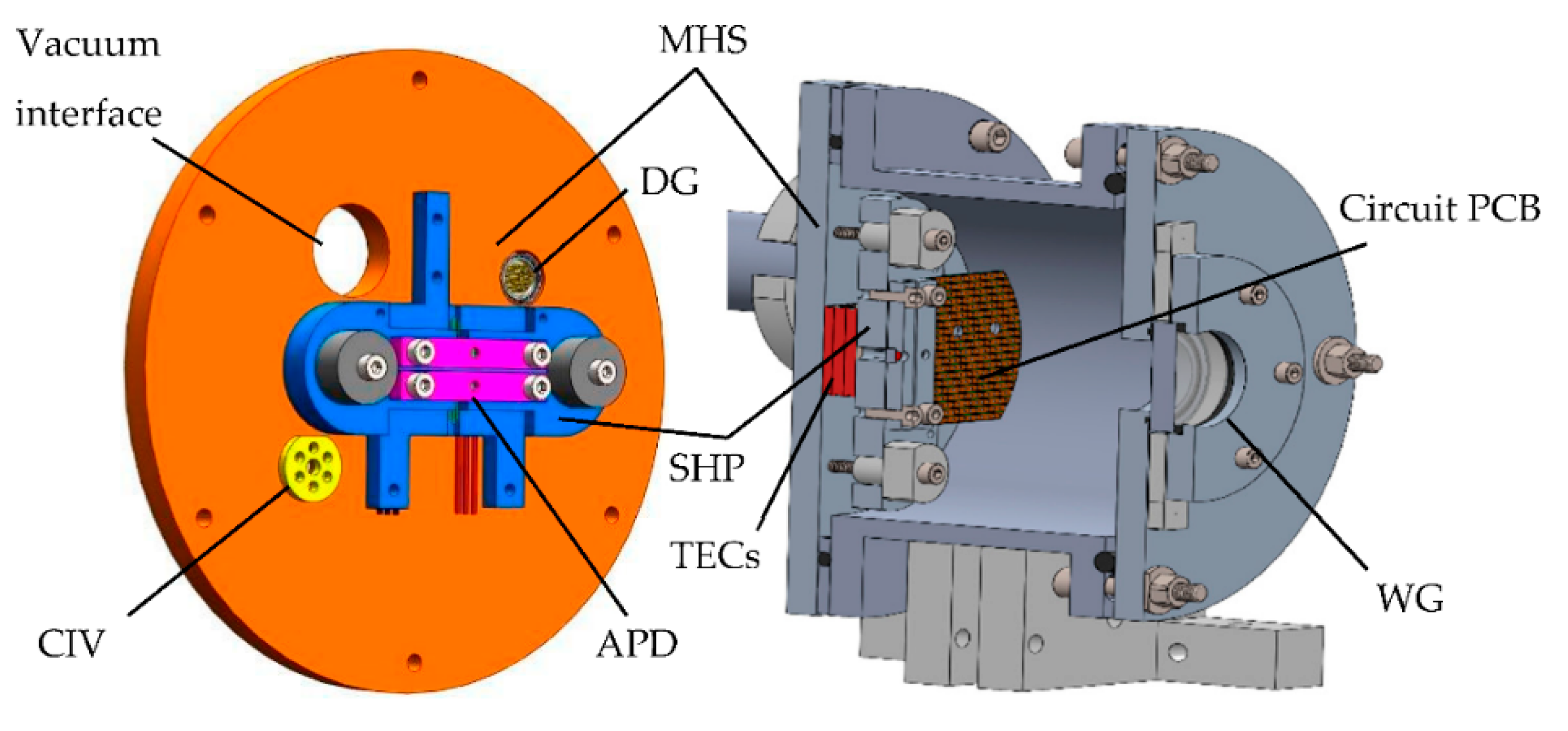
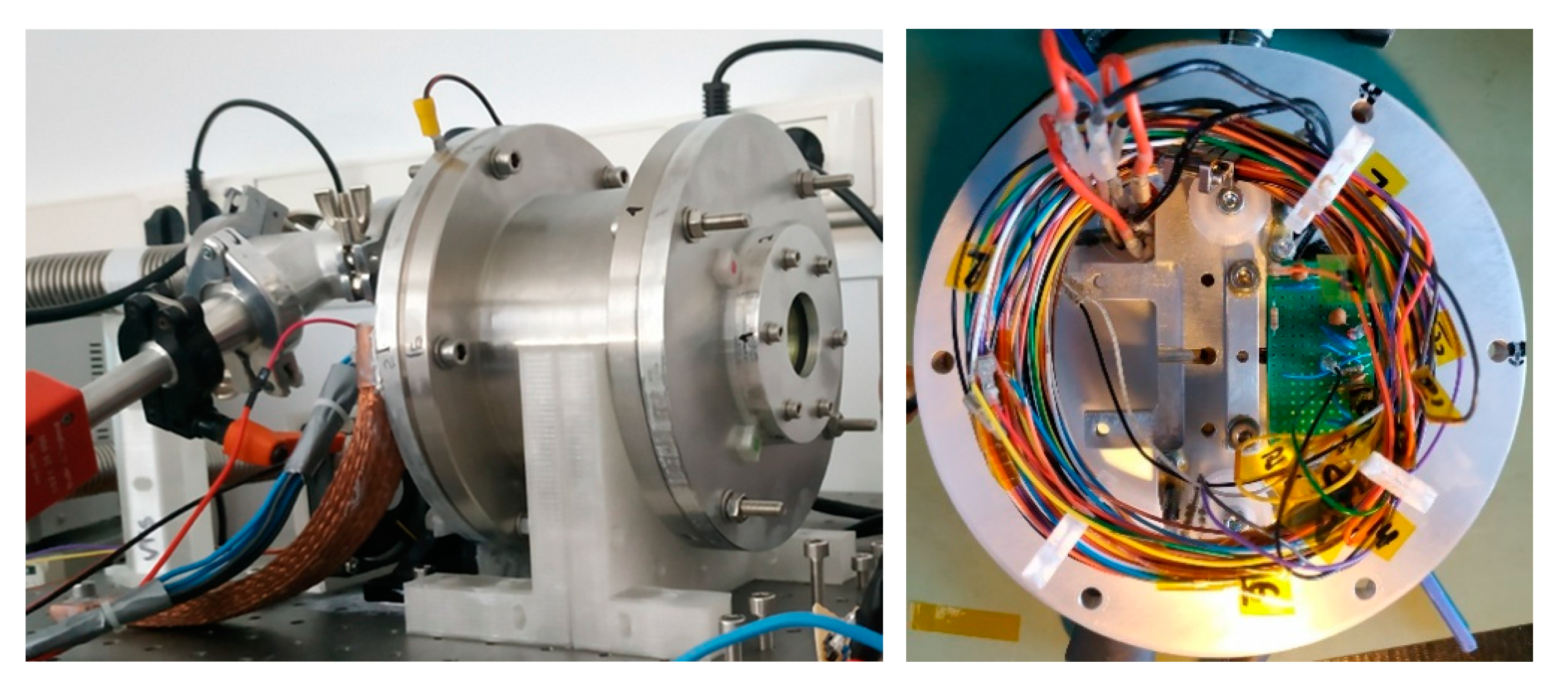
To avoid water vapor condensation at negative temperatures, the APD was tested in a vacuum environment. To achieve this, a test vacuum chamber was designed and manufactured in our laboratories. It consisted of a main body made from stainless steel with a Viton O-ring sealant on one of the extremities, an aluminum main heat sink (MHS), a broadband precision window (N-BK7 WG11508-C coated) (WG), and a sensor holder plate (SHP). Three high performance TECs were positioned between the MHS and SHP.
The temperature was monitored with two 10 kΩ negative temperature coefficient thermistors, one positioned near the sensor and the other on the MHS. The electric interfaces (air-vacuum) were a DEE-Glenair (DG) connector to supply the circuits and the thermistors and a high-power electric interface to power the three TECs current-voltage connector (CIV).
Outside the vacuum chamber, attached to the MHS, were two copper braids connected to an optical table to help dissipate the heat. There was a fourth TEC between the MHS and a smaller second heat sink attached to the optical table, cooled by a small 12 V fan. The chamber walls were covered by multi-layer insulation (MLI) (6 by-layers) to further provide thermal insulation for the sensor. Coupled with the chamber window, there was a ML925B45F Mitsubishi laser diode (LD), operating at 1550 nm, to inject a radiant flux into the chamber. The test setup chamber CAD design and its components can be seen in
Figure 8.
Initial tests performed with a vacuum enclosure showed that the system could sustain vacuum environments as low as 7.4 Pa and stable temperature values on the holder plate from 324 K down to 243 K, thus achieving the necessary conditions to test the sensors. The image of the chamber fully manufactured is provided in
Figure 9.
3.2. Test Circuits
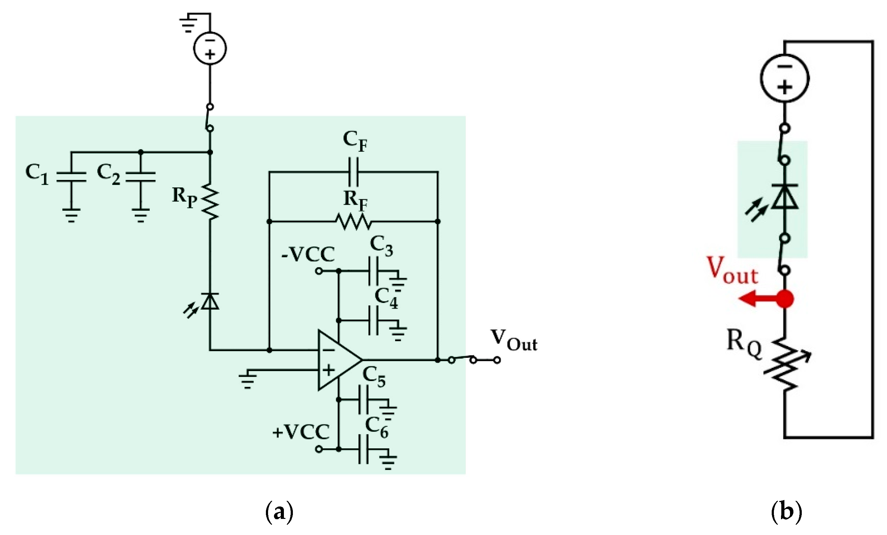
Two circuits for the sensor biasing and readout electronics were implemented and tested: a TIA and a PQC.
The voltage signal produced by the TIA circuit was directly monitored on an oscilloscope for various test conditions, including changing environmental temperature, photodetector bias, and radiant flux. The system signal gain resulted from the multiplication of the APD gain and the TIA gain, determined by the amplifier feedback resistor.
The configuration of the PQC circuit considered a quenching resistor to determine the amount of de-biasing produced when the avalanche occurs and the photodetector is draining large current levels. This effect drives the photodetector out of the avalanche regime and back to a lower gain in linear mode. A second aspect affecting the choice of the quenching resistor is the circuit time constant, mainly determined by the values of and the . This limits the circuit dead time and thus the capability of the detection circuit to be able to respond to two closely separated optical pulses.
The two types of circuits used are depicted in
Figure 10, with the respective components used. Their values were scaled according to the circuit dimensioning equations to meet certain requirements for the tests conducted in the labs. We added to the TIA circuit a protection resistor,
.
The TIA circuit was attached to the sensor holder plate inside the chamber, while the PQC was used outside the vacuum environment for flexible adjustment of the quenching resistor value.
3.3. TIA Results
The TIA circuit’s (
Figure 10a) maximum output voltage was limited by the operational amplifier power supply, which was set to
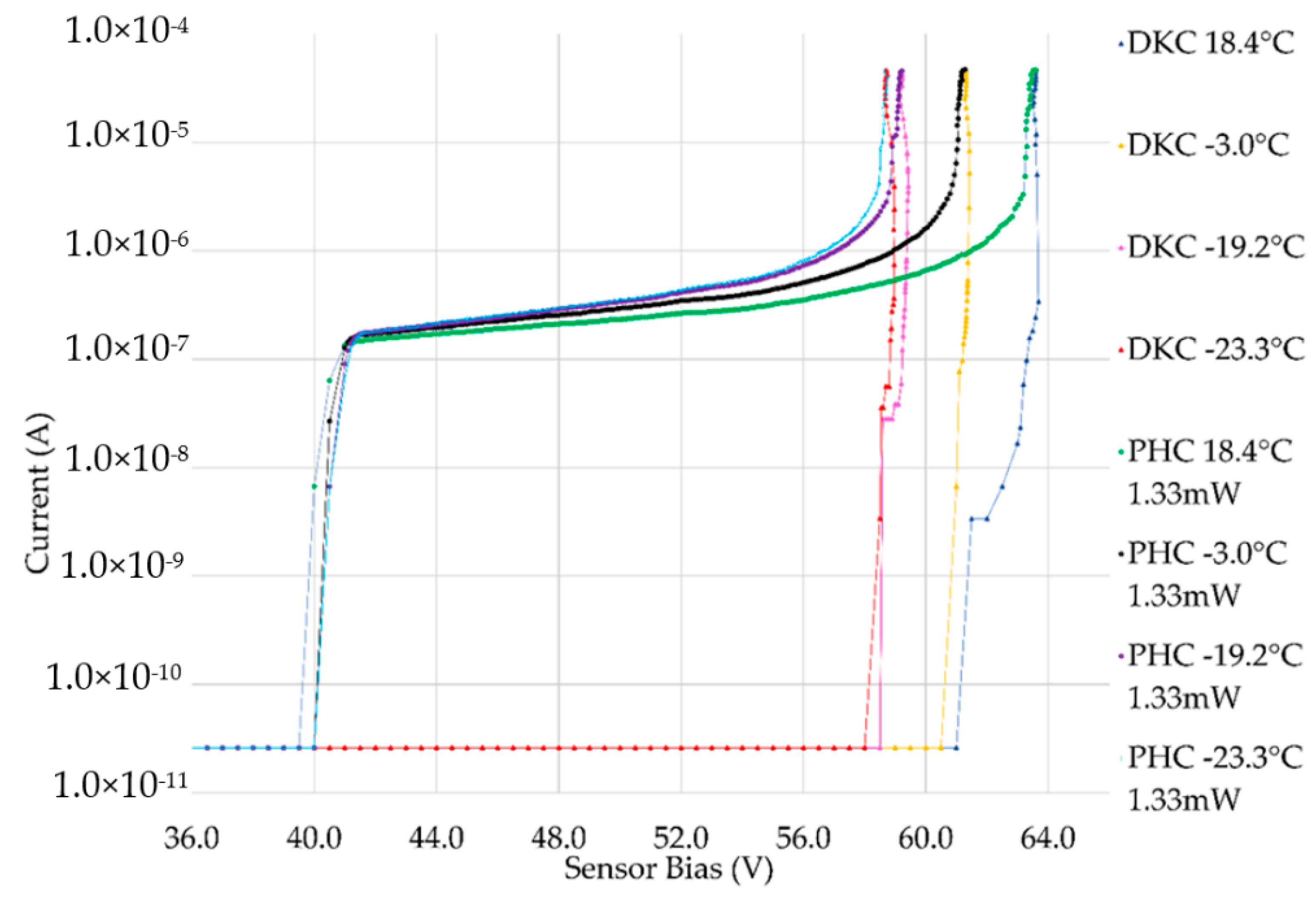
. Using this circuit, the APD was characterized for four different temperatures: −23.3 °C, −19.2 °C, −3.0 °C, and 18.4 °C. The characterizations comprised the measurements of the dark current (DKC) and photocurrent (PHC). For the photocurrent measurements, the APD was exposed to a 1.55 µm CW diode laser operating at different optical powers: 0.03 mW, 1.30 mW, and 3.00 mW.
The laser was positioned in front of the vacuum chamber window, pointing directly at the sensor. Due to the laser’s divergence, its distance from the sensor, and its small sensor area, only a small fraction of its power is detected by the sensor. A rough estimation of the optical power reaching the sensor active area can be made knowing that the distance from the center of the laser diode window up to the APD window was 110.8 mm, the laser diode beam divergence (FWHM) is 25° parallel and 30° perpendicular, and considering the optical powers for the given wavelength. The total incident power was estimated to be 4.11 × 10⁻⁸ W, 1.82 × 10⁻⁸ W, and 4.11 × 10⁻¹⁰ W, for 3.00 mW, 1.33 mW, and 0.03 mW, respectively. In the next figures, the measurement results obtained while operating the laser at 1.33 mW are presented.
The data using an optical power of 1.33 mW for 4 different temperatures is plotted in
Figure 11. The shift of the IV curves is noticeable for the different working temperatures, as the gain increases more significantly at lower bias voltages as temperature decreases. The same analysis was made for an optical power of 3.00 mW and 0.03 mW, with similar behavior being observed.
In
Figure 11, all the data points end at 4.7 × 10
−5 A, which represents the peak current value for each dataset, limited by the chosen operational amplifier and gain. Note that the current produced by the sensor is not exclusively generated by the optical power. Instead, it includes mutually the contributions of the dark current and the photogenerated current, both multiplied by the photodetector gain. For this reason, it is necessary to subtract the photocurrent values from the dark current measurements in order to calculate a “true” effective photocurrent. In this way, it was possible to estimate the photocurrent produced by incident optical power alone [
27].
This allowed the calculation of the avalanche photodiode gain for the different optical powers and temperatures. The gain was given by the ratio of the effective photocurrent and the primary effective photocurrent.
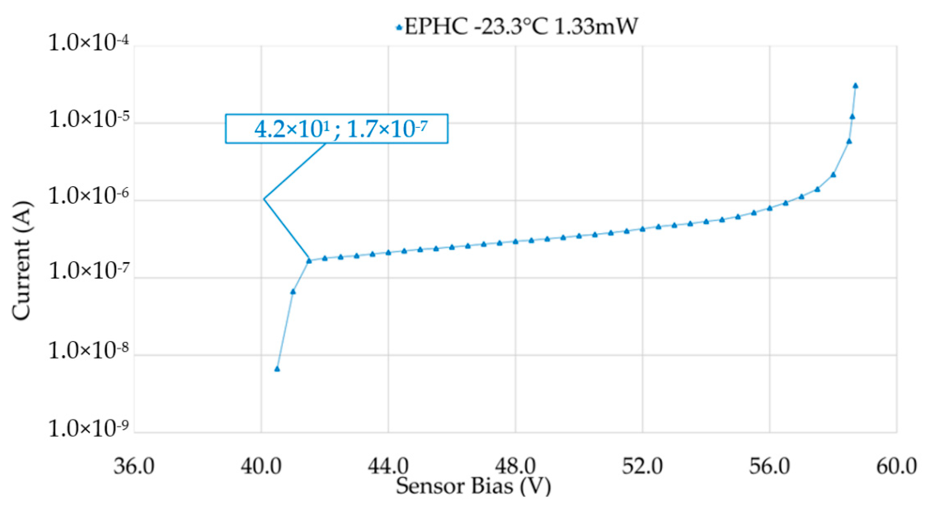
The calculated gain values are strongly dependent on the value of the primary effective photocurrent used. To choose the best primary effective photocurrent, we considered the punch-through current as the primary effective current value, defined as the photocurrent corresponding to gain = 1 when the punch-through voltage is reached. In this condition the layers responsible for the photon detection and triggering the avalanche effect are fully depleted [
28]. By plotting the effective current in function of the sensor bias, the punch-through voltage is met when a (first) noticeable increase in the effective photocurrent occurs and a consequent, almost constant, current increase follows, for roughly 1 V to 2 V in the variation of the APD bias. An example of the choice of this current value is shown in
Figure 12.
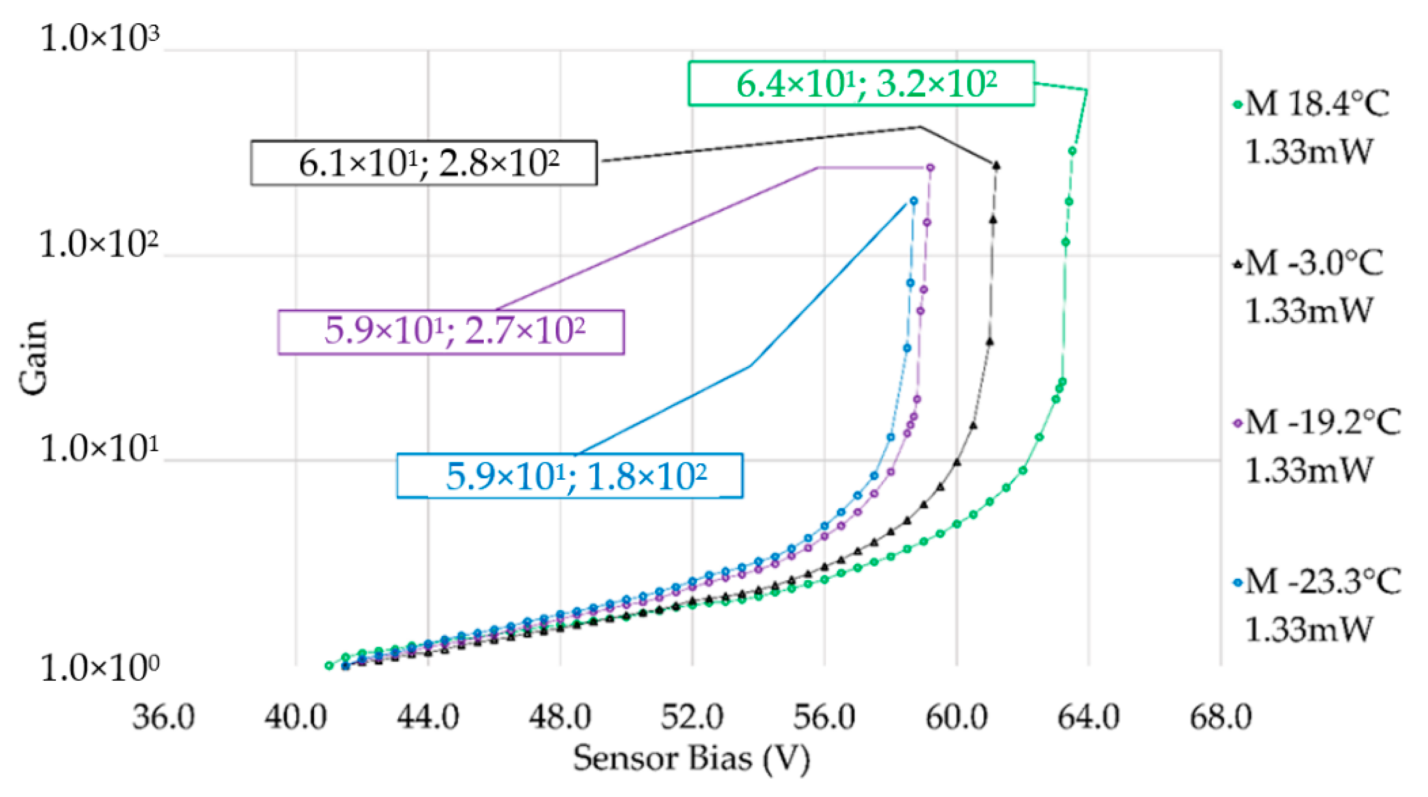
The calculated gain utilizing the effective photocurrent (EPHC) value for the four different temperatures is presented in
Figure 13.
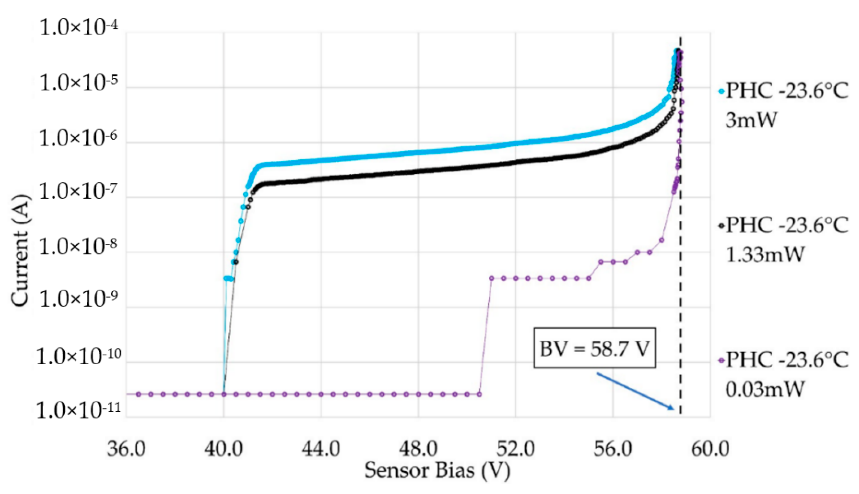
In
Figure 13, the highest gain reachable is shown is 346.1 for 18.4 °C and 184.3 for −23.3 °C. The APD was operated in avalanche mode with sustained high gains, much higher than the ones reported in the datasheet (in the datasheet, the APD is only operated up to gains = 40). For the −23.3 °C, the breakdown voltage was reached at 58.7 ± 0.1 V (cathode/anode voltage), but not crossed, due to saturation of the TIA APD. These can be seen in
Figure 14; therefore, Geiger mode operation was not reached.
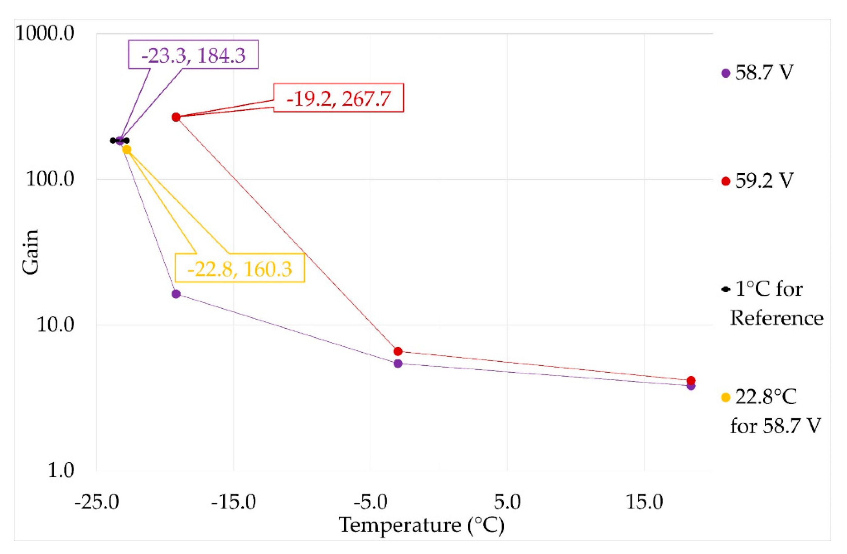
To operate the APD at these high gains, it is important to have an accurate temperature control since a temperature variation can induce a high variation in the gain.
Figure 15 gives the gain variation as a function of temperature. As an example, for a bias of 58.7 V, the gain varies more than 40 times for temperatures ranging from 22 °C to −23 °C, showing that a fine temperature control is needed.
In
Figure 15, it is possible to see that by decreasing the temperature at −23.3 °C by half a degree, the gain for a polarization of 58.7 V is reduced by roughly 24.
3.4. PQC Results
When applying and testing the PQC circuit, it was realized that the impact of the quenching resistor value not only applies to the time constant constraints but also to the actual photodiode output voltage magnitude. Low resistor values are better for reaching higher polarizations due to the low drain voltage drop across them, but it also means that the output voltage values measured (on the red tag indicated in
Figure 10b) are very small, thus needing increased readout resolution.
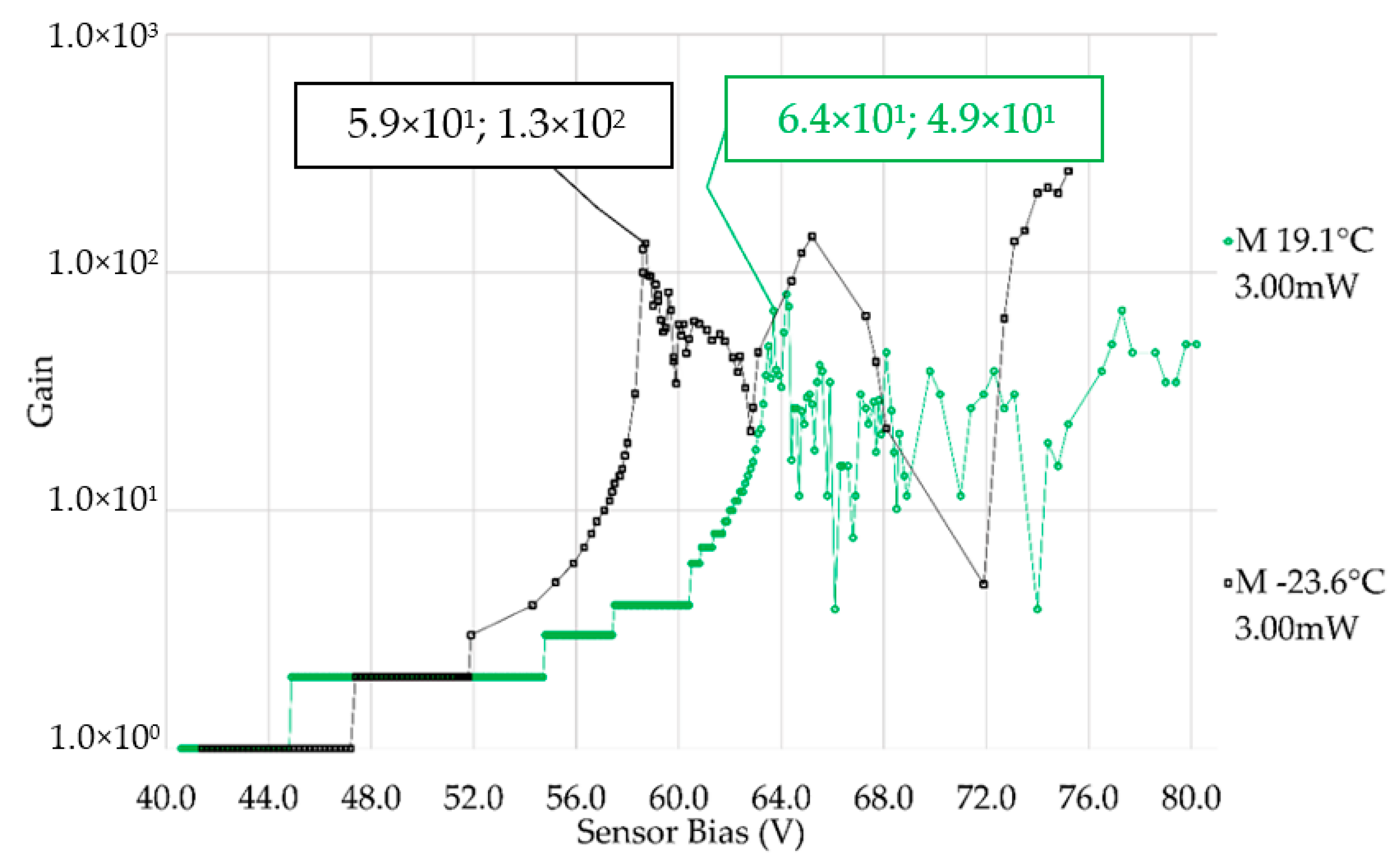
For this circuit, various values of quenching resistors were implemented and tested, from megaohms to a few ohms, to understand the concepts mentioned above. For the results reported here, the laser diode was set to an optical power of 3 mW, and three different quenching resistors, 54.50 kΩ, 9.79 kΩ, and 5.5 kΩ, were used.
Due to the oscilloscope resolution, using resistor values below 5 kΩ made the reading of the output voltage difficult (in accordance with what was mentioned above), while the maximum safety current value for the photodiode was quickly reached using the same source bias steps as for the other two resistors.
Using the mean output voltage measurements, an IV graphic was plotted for the PQC. This was conducted using the same principles employed for the TIA circuit in
Figure 11. For better clarity to the reader, only the dark current values and photocurrent values of the 9.79 kΩ are shown in
Figure 16.
The four data labels in
Figure 16 indicate the bias values for which a current of about 2 mA is reached for the different temperatures and lighting conditions. As shown in this figure, the behavior of the sensor remains comparable to the data obtained when using the TIA circuit (
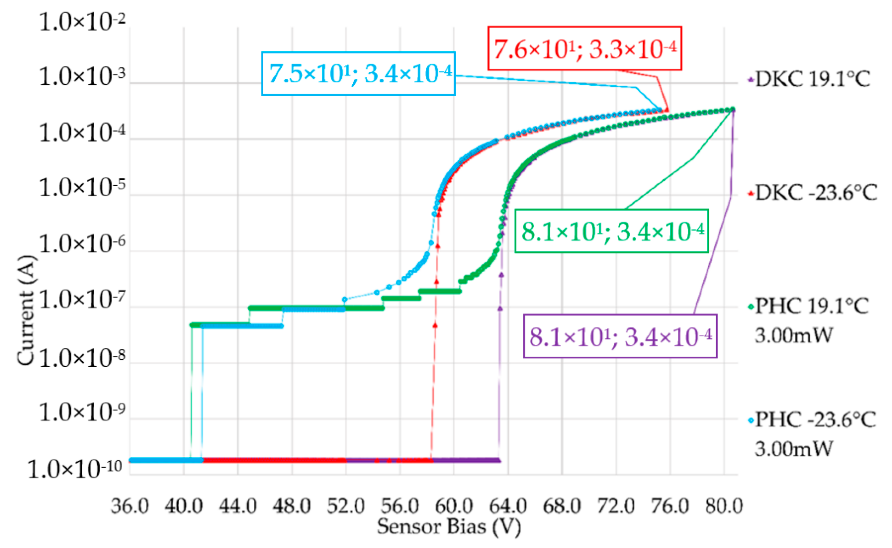
Figure 11). Above that region, the current shows a saturation behavior and varies negligibly even with a bias voltage increase of about 15 V.
By computing the dark current data for the three resistors used, it was found that the Geiger mode region was well achieved. In fact, all the dark current values retrieved reached near 2 mA, much further than the 100 µA threshold assumed as the frontier between the avalanche and Geiger regions. From the highest resistance to the lowest, for the temperatures of 19.1 °C and −23.6 °C, the breakdown voltage values found are as follows: 63.6 V and 58.6 V; 68.5 V and 64.0 V; 69.3 V and 64.4 V, respectively. With the breakdown voltage data for at least two temperatures, one can then calculate the temperature coefficient of breakdown voltage, β, uniformly giving 0.11 V/°C for the three resistors and matching the value provided by the datasheet.
To calculate the gain, the primary effective photocurrent was selected by the same method used for the TIA. This, once again, greatly impacts the gain values calculated. Like before, only the data using the 9.79 kΩ resistor is plotted for better visualization.
A distinct behavior of the one seen in the gain curves extracted with the TIA circuit (
Figure 13) can be seen comparing it with the one made by using the PQC (
Figure 17), which allowed to push the sensor up to its current limit (i.e., above breakdown voltage). After a certain bias value, highlighted by the data labels, the gain is no longer sustained, behaving erratically even for very small bias variations. This can be explained by the effects of the depolarization (and the consequent recuperation, thus lowering the gain briefly) imposed by the quenching resistor due to the high generated currents. Combining this with the competitive behavior between the multiplied photocurrent and the multiplied dark current and keeping in mind that the sensor was not designed internally for Geiger mode use, the chaotic nature of the Geiger mode region and avalanche region limit can be well noticed. For the other two resistors, similar behavior occurs.
PQC Pulsed Laser Results
To detect and see on the oscilloscope the quenching behavior of the signal, the oscilloscope needs to have a certain sample rate, enough to distinguish the peak and relaxation behavior of the continuous averaged signal. Aside from all the considerations made before, the PQC is the simplest circuit to both measure and protect the avalanche photodiodes from damage while having a simple control of their photon detection rate.
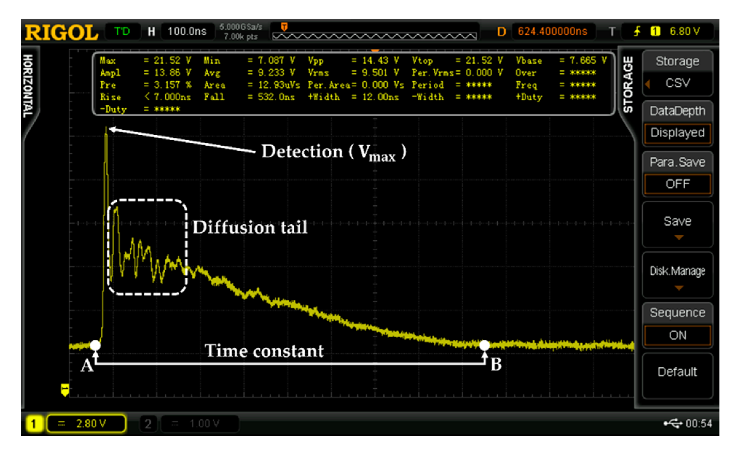
By changing the continuous wave laser diode for a pulsed laser with higher optical power using the same three resistors for the PQC, it was possible to see a detection peak and the consequent relaxation behavior due to the resistor effect.
Figure 18 illustrates this detection with visible afterpulsing, and the recuperation time between the points A and B with a sensor bias of 56.4 V. In
Figure 18, the values shown as “*****” are due to the inability of the oscilloscope to measure certain values.
4. Summary and Conclusions
In the scope of the development of LiDAR for space applications concerning volume, power consumption, and performance, we presented in this work our studies and experiments associated with the development of two key components of a LiDAR, namely a microchip laser and an avalanche photodiode sensor. The synergy of these components would be an initial approach to the development of LiDAR with low power consumption and dimensions.
The work performed for the microchip laser as the light emitter of the LiDAR resulted in four optical cavities with different characteristics. Their slope efficiencies ranged from 6% to 16%. All cavities emitted wavelengths around 1532 nm. The optical cavity with pulsed emission chosen for the fixed optical cavity had a slope efficiency of 8.5%. It had burst emission, with micro-pulses with over 30 µJ of pulse energy, 11.6 ns of pulse width, and over 3 kW of optical peak power.
The design presented for the fixed optical cavity made it possible to fix an optical cavity with CW emission with a slope efficiency of 16.7%. The Q-switching operation was, however, not achieved in a fully assembled laser mount, mainly due to the intricacies of the gluing process. The glue itself presented the problem of contracting during the cure time, which changed the alignment of the optical component being glued.
For the receiver end of the LiDAR, the tests performed on the APD are the initial fundamental steps for the characterization and optimization of this type of sensing system, with maximum sustained gain in conditions close to those experienced in space. The implemented TIA circuit allowed a more stable operation of the APD at high gains at lower bias voltages when compared with the PQC results, thus favoring conditions for a lower power consumption solution.
In conclusion, the solutions studied for the two key components presented in this work are leading to an overall LiDAR architecture based on a miniaturized high peak power microchip laser associated with a receiver solution based on a high sustained gain avalanche sensor that supports the development of equipment enduring the predicaments of space operation.


 ,
, 


