
Structural Decomposition in FSM Design: Roots, Evolution, Current State—A Review


1
Institute of Metrology, Electronics and Computer Science, University of Zielona Góra, ul. Licealna 9, 65-417 Zielona Góra, Poland
2
Department of Mathematics and Information Technology, Vasyl’ Stus Donetsk National University, 600-richya str. 21, 21021 Vinnytsia, Ukraine
3
Department of Infocommunication Engineering, Faculty of Infocommunications, Kharkiv National University of Radio Electronics, Nauky Avenue 14, 61166 Kharkiv, Ukraine
4
Department of Technology, The Jacob of Paradies University, ul. Teatralna 25, 66-400 Gorzów Wielkopolski, Poland
*
Author to whom correspondence should be addressed.
Electronics 2021, 10(10), 1174; https://0-doi-org.brum.beds.ac.uk/10.3390/electronics10101174
Submission received: 14 April 2021
/
Revised: 29 April 2021
/
Accepted: 12 May 2021
/
Published: 14 May 2021
(This article belongs to the Special Issue 10th Anniversary of Electronics: Advances in Circuit and Signal Processing)
Abstract
:The review is devoted to methods of structural decomposition that are used for optimizing characteristics of circuits of finite state machines (FSMs). These methods are connected with the increasing the number of logic levels in resulting FSM circuits. They can be viewed as an alternative to methods of functional decompositions. The roots of these methods are analysed. It is shown that the first methods of structural decomposition have appeared in 1950s together with microprogram control units. The basic methods of structural decomposition are analysed. They are such methods as the replacement of FSM inputs, encoding collections of FSM outputs, and encoding of terms. It is shown that these methods can be used for any element basis. Additionally, the joint application of different methods is shown. The analysis of change in these methods related to the evolution of the logic elements is performed. The application of these methods for optimizing FPGA- based FSMs is shown. Such new methods as twofold state assignment and mixed encoding of outputs are analysed. Some methods are illustrated with examples of FSM synthesis. Additionally, some experimental results are represented. These results prove that the methods of structural decomposition really improve the characteristics of FSM circuits.
Keywords:
finite state machine; synthesis; microprogram control unit; logic elements; structural decomposition; PROM; PLA; PAL; CPLD; FPGA1. Introduction
The development of information technologies has led to the widespread use of various digital systems in different areas of mankind’s activity [1,2,3,4,5,6,7,8,9]. It is known that digital systems consist of various combinational and sequential blocks [10,11]. As a rule, the circuits of combinational blocks are regular [12]. A designer can use standard library elements of computer-aided design (CAD) systems to implement such circuits [11]. For example, a multi-bit adder can be represented as a composition of standard single-bit adders. The sequential blocks could be very complex (for example, control units of computers) or rather simple (such as binary counters). It is known that the circuits of complex sequential blocks are irregular [10,12]. As a rule, there are no standard library solutions for such blocks. It means that each sequential block is synthesised anew. To synthesise the logic circuit of a sequential block, some tools are used to present the law of its behaviour.
Very often, the behaviour of sequential blocks is represented using the model of a finite state machine (FSM) [10,13,14]. Three characteristics of an FSM circuit significantly influence the characteristics of a digital system. These characteristics are the hardware amount, the operating frequency (the performance), and the power consumption. Because of it, there is continuous interest in developing the various approaches that aimed at optimizing the basic characteristics of FSM circuits. As a rule, the less hardware is consumed by a sequential block’s circuit, the less power it requires [15,16,17,18,19,20]. Accordingly, it is very important to reduce the amount of hardware that is consumed by an FSM circuit.
The development of various methods of optimizing the characteristics of the FSM circuits has been started since 1951. A characteristic feature of such methods is the consideration of the characteristics of the logic elements that are used for the design of FSM circuits. At various times, various logic elements were used for implementing FSM circuits. Among these elements, there are logic gates, decoders, multiplexors, read-only memories (ROMs), programmable ROMs (PROMs), programmable logic arrays (PLAs), programmable array logic (PAL), complex programmable logic devices (CPLDs), and field-programmable gate arrays (FPGAs). Some of these logic elements have been used together.
The structural decomposition is one of the approaches used for reducing the hardware amount [21,22,23,24]. The roots of this approach go back to 1951, when M. Wilkes put forward the idea of a microprogram control unit (MCU) [25,26]. Over the following times, Wilkes’ ideas were modified with a change in the elemental basis used for implementing FSM circuits.
The main idea of the structural decomposition is the following. An FSM circuit is represented by some big logic blocks. Each such a block has its own unique input variables and output functions. The outputs of some blocks are used as the inputs of other blocks. This allows for eliminating the direct connection between FSM inputs and outputs. In the best case, the logic circuit of each block has exactly a single level of logic elements [21,27,28]. In this article, we present a rather brief survey of the known methods of structural decomposition. At the same time, almost half of the article is devoted to the methods of structural decomposition used for optimizing the circuits of FPGA-based FSMs.
The main contribution of this paper is a survey of methods of structural decomposition of FSM circuits. The analysis of these methods shows that the structural decomposition is a powerful tool that allows for significantly improving the characteristics of FSM circuits as compared to their counterparts based on other known approaches.
The rest of the paper is organized as the following. Section 2 presents the theoretical background of finite state machines. Section 3 discusses the methods of implementing microprogram control units. Section 4 presents the methods of structural decomposition used in application-specific integratedcircuits. Section 5 considers the methods targeting simple programmable logic devices. Section 6 considers the structural decomposition of FPGA-based FSMs. A brief conclusion ends the paper.
2. Implementing Circuits of Finite State Machines
An FSM can be defined as a tuple [10,13], where is a set of internal states, is a set of inputs, is a set of outputs, is a transition function, is a function of output, and is an initial state. An FSM can be represented using such tools as: state transition graphs [10], binary decision diagrams [29], and-inverter graphs [30], graph-schemes of algorithms [13].
The most obvious way to represent an FSM is the state transition graph. For example, the STG that is shown in Figure 1 represents a Mealy FSM .
The FSM states are represented by the nodes . The arcs define the interstate transitions that are determined by the input signals that are the conjunctions of inputs (or their complements). These conjunctions are written above the arcs together with the outputs generated during these transitions. Using STG (Figure 1), we can find the following parameters of Mealy FSM : the number of inputs , the number of outputs , the number of states , and the number of transitions . Additionally, this STG uniquely defines the functions of transitions and output of FSM .
To design an FSM circuit, an STG should be transformed into the corresponding STT. An STT includes the following columns [10,13]: is a current state; is a state of transition; an input signal determining a transition from to ; and, is a subset of the set of outputs generated during the transition from the current state to the state of transition . We name this subset a collection of outputs. The numbers of the transitions () are shown in the last column of the STT.
In this article, we mostly use STTs for initial representation of FSMs. For example, the FSM is represented by the STT (Table 1). We hope that there is the transparent connection between the STG (Figure 1) and STT (Table 1).
There are two main types of FSM, namely, Mealy [31] and Moore [32] FSMs. The first of them was proposed in 1955 by G. Mealy; the second was proposed in 1956 by E. Moore. In both cases, the function determines the states of transition as functions depending on the current states and inputs. So, it is the following function:
For Mealy FSMs, the function determines the outputs as functions depending on the current states and inputs. It gives the following function:
For Moore FSMs, the function determines the outputs as functions depending only on the current states. So, it is the following function:
The difference among (2) and (3) leads to a difference in the synthesis methods of Mealy and Moore FSMs. We now explain the stages of Mealy FSM’s synthesis starting from Table 1.
In 1965, Viktor Glushkov proved a theorem of the structural completeness [33]. According to this theorem, an FSM circuit is represented as a composition of the combinational part and the memory. The memory is necessary for keeping the history of the FSM’s operation. The history is represented by FSM internal states. This fundamental approach is still widely used for the synthesis of FSM circuits [34,35,36,37,38].
An FSM logic circuit is represented by some systems of Boolean functions (SBFs) [10,13]. To find these SBFs for Mealy FSMs, it is necessary to [13]: (1) encode states by binary codes ; (2) construct sets of state variables and input memory functions (IMFs) ; and, (3) transform an initial STT into a direct structure table (DST). The states are encoded during the step of state assignment [10].
The minimum possible number of state variables is determined as
The approach based on (4) defines so-called maximum binary codes [10]. This method is used, for example, in the well-known academic system SIS [39]. However, the number of state variables can be different from (4). For example, the one-hot state codes with are used in the academic system ABC [30,40] of Berkeley. The maximum binary codes and one-hot codes define the extreme points of the encoding space. There are other approaches for state assignment where the following relation holds: .
A state register (RG) keeps the state codes. The register includes R memory elements (flip-flops) having shared inputs of synchronization (Clock) and reset (Start). Very often, master–slave D flip-flops are used to organize state registers [41,42]. The pulse Clock allows the functions to change the RG content.
After the execution of the state assignment, we should create a direct structure table. A DST includes all of the columns of an STT and three additional columns. These columns include the current state codes and the codes of the states of transitions. Finally, a column includes the symbols corresponding to 1’s in the code from the row h of a DST (). A DST is a base to construct the following SBFs:
The block of input memory functions generates the functions (5). The block of outputs generates the system (6). The pulse Start loads the code of the initial state to RG. The pulse of synchronization Clock allows information to be written to the register.
A DST of Moore FSM is a base for deriving the systems (5) and
A P Moore FSM is represented by a structural diagram that is similar to the one shown in Figure 2. However, as follows from SBF (7), there is no connection between the inputs and block of outputs.
We now discuss how to obtain systems (5) and (6) for P Mealy FSM . There is . Using (4) gives the value of . This determines the sets and . Let us encode states in the trivial way: . Having state codes allows transforming Table 1 (the initial STT) to Table 2. Table 2 is the DST of P FSM .
To fill the column , we should take into account that the value of is equal to the value of the r-th bit of code [13]. Systems (5) and (6) are represented as a sum-of-products (SOPs) [10,43]. These SOPs include product terms corresponding to rows of a DST. The elements of the set of terms F are determined as
In (8), the first member is a conjunction of state variables corresponding to a code of the current state from the h-th row of DST. There are the following conjunctions in the discussed case: .
The SBF (9) determines the circuit of block of outputs and the SBF (10) determines the circuit of block of input memory functions.
The hardware amount in an FSM circuit depends on the combination of SBF characteristics (the numbers of literals, functions, and product terms of SOPs) and specifics of the used logic elements (the number of inputs, outputs and product terms). Denote, by , the number of literals in a term of the SOP of a function , and, by , the number of terms in a SOP of this function. Obviously, the following conditions are true for a SOP of any function :
Consider the SOP of function from SBF (10). Each term of this SOP includes literals. There are terms in this SOP. If NAND gates having inputs are used for implementing a logic circuit corresponding to , then there are four gates and two levels of gates in the circuit. This is the best solution, because the circuit includes the minimum possible number of gates (the minimum hardware amount), their levels (the maximum operating frequency), and interconnections.
However, if there is , then the SOP should be transformed. After the transformation, the SOP is represented by the following formula:
Twelve gates are necessary for implementing the function (13). The resulting circuit has six levels of gates. Thus, an imbalance between the characteristics of the function and logic elements leads to an increase in the number of gates and levels of logic in the resulting logic circuit.
This situation can occur for any logical elements (logic gates, ROMs, PROMs, PLAs, PALs, CPLDs, FPGAs, and so on). In this case, it is necessary to optimize the characteristics of a resulting logic circuit. The structural decomposition is one of the ways for such an optimization [21].
3. Roots of Structural Decomposition
The control units’ circuits of the first computers were characterized by an irregular structure [45,46,47,48] with all the ensuing consequences. In 1951, Professor of Cambridge M. Wilkes proposed a principle of microprogram control [25,26]. According to this principle, each computer instruction is represented as a microprogram kept into a special control memory (CM). A microprogram consists of microinstructions. Each microinstruction has an operational part with control outputs (microoperations) and an address part having data used for generating an address of transition (the address of the next microinstruction to be executed). A special register is used to keep the microinstruction address. This approach allows for obtaining a microprogram control unit (MCU) with a regular circuit, which is quite simple to implement and test. A trivial structural diagram of the MCU is shown in Figure 3.
The MCU (Figure 3) uses the microinstruction address from the register and logical conditions (inputs) to generate outputs and the next address represented by variables . A comparison of Figure 2 and Figure 3 shows that the MCU is a finite state machine in which blocks of input memory functions and outputs are replaced by the control memory. At the same time, microinstructions correspond to FSM states; microinstruction addresses correspond to state codes. This connection between FSMs and MCUs was first noted in [49].
The circuit of control memory was implemented using ROM [50,51,52]. For MCU (Figure 3), the required volume of such a ROM, , is determined as
For average FSMs [13], there is . If such a control unit is implemented as MCU (Figure 3), then it is necessary for bits of control memory. In the 1950s, the use of such a big control memory would lead to a significant increase in the cost of a computer. Because of it, Figure 3 rather shows an idea of MCU, not the practical way of its implementation.
In order to diminish the required value of , two approaches have been proposed by M. Wilkes. The first of them is the selection of an input that should be used for generation of the transition address. As a rule, only a single logic condition is selected in each cycle of MCU operation. This allows for reducing the length of the address part of microinstruction. This approach leads to a two-level MCU shown in Figure 4.
The second approach is an encoding of collections of microoperations by maximum binary codes having bits. In practical cases [53], there is . This allows reducing the length of the operational part of microinstruction up to
In (15), we use Q to denote the number of different COs for a particular STT.
If an MCU is implemented starting from STT (Table 1), then the following collections of outputs (COs) can be found: , , , . Accordingly, there is . Using (15) gives . Let us use elements of the set for encoding of the COs. It gives the set . Figure 5 shows one of the possible outcomes of encoding.
As follows from Figure 5, there is . The system of outputs is represented by the following SOP:
To implement the system (16), we should include in the MCU a block of outputs. This block consists of a decoder (DC) and a coder. Hence, this block has two levels of logic. The decoder transforms codes of COs into one-hot codes corresponding to COs. The coder transforms these one-hot codes into outputs. In the general case, the outputs are represented by the system
If both of the approaches are used simultaneously, then there are three levels of logic blocks in the MCU. Figure 6 shows the structural diagram of three-level MCU with the compulsory addressing of microinstructions [50,54].
In the case of the compulsory addressing of microinstructions, the microinstruction format includes the operational part having bits and the address part having bits with a code of logical condition to be checked and two address fields. The first address field includes an address of transition, if a logical condition to be checked is equal to 0 (or an address of unconditional transition). The second address field includes an address of transition if a logical condition to be checked is equal to 1. If a microprogram includes M microinstructions, then the number of address bits is determined by (4). Accordingy, each microinstruction has bits. If and , then the value of is equal to bits.
The block of addressing generates address variables . These variables depend on the inputs and microinstruction address part. This block is implemented on multiplexers (MXs) [52]. The block of outputs generates outputs as functions of the MCU operational part. Hence, an MCU is a Moore FSM.
The MCU with the block of addressing became the prototype of the FSMs with replacement of inputs. In literature [41] such FSMs are called FSMs, where “M” means “multiplexer”. The MCU with the block of outputs became the prototype of FSMs with encoding of collections of outputs. The three-level MCU (Figure 6) corresponds to FSM. This means that various methods of structural decomposition can be used together.
The method of encoding of fields of compatible outputs (FCOs) was proposed to eliminate the coder from the block of outputs [55]. The outputs are compatible if they are not written in the same rows of STT. The set O is divided by I classes of compatible outputs:
Outputs are encoded by maximum binary codes . There are bits in the code :
In (19), we use the symbol to denote the number of outputs in the class . The one is added to to take the relation into account.
The outputs are encoded using variables . The total number of operational part bits, , is determined by summation of the values of (19). The structural diagram of the MCU based on this principle is the same as the one shown in Figure 6. However, the block of outputs consists of I decoders . A decoder generates outputs from the field .
This approach was used in optimizing control units of IBM/360 [56]. Additionally, they became the prototypes of FSMs [41].
There are three possible organizations of the block of outputs that are shown in Figure 7.
As follows from Figure 7, the one-hot organization (Figure 7a) leads to the fastest MCUs having the longest operational part. The block of outputs is absent. The maximum encoding of collections of outputs (Figure 7b) results in the two-level block of outputs. This is the slowest solution, but it provides the shortest operational part. As follows from Figure 7c, the encoding of FCOs results in a single-level block of outputs. This approach provides a compromise solution with the average delay and hardware amount.
The value of can be reduced due to using the nanomemory [44,54]. We now explain the idea of this approach (Figure 8).
If there are unique microinstructions in a microprogram, then they are encoded using variables , where is determined as it is for . These codes are kept into a micro-memory (the first level of control memory). There are M codes in the micro-memory. The second level of memory (nanomemory) keeps the operational and addresses parts of these microinstructions. For example, there is , , and a microinstruction contains 64 bits. In the case of MCU (Figure 6), there are bits. We have . Accordingly, there are bits of the micro-memory and bits of the nanomemory. Hence, there are 26,624 bits of the control memory for MCU (Figure 8). It means that that approach allows reducing the volume of control memory by 2.46 time when compared to the MCU (Figure 6). This approach is a prototype of FSMs with encoding of product terms [41].
One fundamental law follows from the analysis of different methods of minimizing the value of . This is the following: the reducing hardware amount leads to an increase in the delay time of the resulting circuit (due to an increase in the number of logic levels). This law holds for all methods of structural decomposition.
4. Structural Decomposition in Matrix-Based Fsms
If an FSM is a part of an application-specific integrated circuit (ASIC) [57], then its circuit can be implemented using custom matrices [13,58]. These matrices are used as either AND-planes or OR-planes [59]. Each plane is a system of wires connected by CMOS transistors. Two wires (direct and compliment values of corresponding arguments) represent each literal of a SOP. Each term of a SOP corresponds to a wire.
To implement a matrix circuit of Mealy FSM, it is enough to use a single AND-matrix and a single OR-matrix . This is a trivial matrix implementation of P Mealy FSM (Figure 9).
The trivial matrix circuit (Figure 9) represents a P Mealy FSM [41]. This is the fastest matrix solution. However, such a solution is very redundant.
The hardware amount of matrix circuits is defined in conventional units of area (CUA) of matrices [13]. These areas are determined as the following:
If there is , , , and (an average FSM [13]), then CUA and CUA. It gives the total area equal to 268,000 CUA. If each product term of SBFs (5) and (6) includes literals, then there are useful interconnections in . If each term enters SOPs of five functions, then there are useful interconnections in . Hence, only 32,000 interconnections are used for implementing an FSM circuit. Because there are 268,000 interconnections, only 12% of the area is really used.
Two methods of structural decomposition were used to reduce the chip area that is occupied by an FSM circuit, namely [58]:
- The replacement of inputs ( FSM).
- The encoding of collections of outputs ( FSM).
To design an FSM, it is necessary to replace the set I by some set . This makes sense if
The value of G is determined by the maximum number of inputs causing transitions from states [58]. Consider the DST of Mealy FSM (Table 3).
In the case of , we have . Accordingly, there is a set .
To replace inputs, it is necessary to create the following SBF:
This SBF is constructed using a table of replacement. In the discussed case, Table 4 presents the table of replacement.
Using Table 4 gives the following SBF:
The SOP for includes terms –; the SOP for includes terms –. Hence, there is .
We should construct a table of FSM to design the circuit of FSM. It can be done by a transformation of the DST of P FSM. The transformation is reduced to the replacement of the column by the column [58]. In the discussed case, this leads to Table 5.
In the Mealy FSM (Figure 10), the matrix implements terms of SBF (23). The matrix transforms terms into functions (23). The matrix implements terms . These terms correspond to the rows of DST. The matrix generates functions (25) and (26). These matrices have the following areas:
To optimize the matrix , the method of encoding of COs can be used [58]. As it is for MCU, Q COs are encoded by binary codes . These codes have bits, where the expression (15) determines the value of .
For FSM , the following COs can be found: , , . Accordingly, there is , , . To minimize the number of literals in (17), it is necessary to encode COs using the approach [60]. In the discussed case, Figure 11 shows the outcome of encoding.
Using codes (Figure 11), we can get the following SBF:
To implement a FSM circuit, it is necessary to create a DST of FSM. For the FSM , it is Table 6.
The DST is a base for deriving SBFs (5) and
In FSM, the matrix implements functions and variables . The matrix transforms into terms of SBF (17). The matrix generates outputs . These matrices have the following areas:
In the matrix circuit (Figure 13), the matrices and implement the SBF (23), the matrices and implement the SBF (17). The matrices and implement SBFs (25) and
There are two levels of logic in the matrix circuit of P Mealy FSM (Figure 9). This circuit has six levels of logic. Obviously, the P FSM is three times faster than an equivalent FSM (Figure 13). Let us compare areas of equivalent FSMs.
As shown in [58], the average FSMs have the following characteristics: , , . This gives the following: , , , , , . Now, we have the following total area of FSM circuit: 83,460 CUA. There are 268,000 CUA of the area of P Mealy FSM (Figure 9). This gives around 69% of economy. Accoridngly, an increase in the number of levels of a matrix circuit leads to an average reduction in area by 3.23 times. Of course, the FSM performance practically decreases to the same extent.
5. Structural Decomposition in Spld-Based Fsms
In the 1970s, a wide range of so-called simple programmable logic devices (SPLDs) appeared. This class includes programmable logic arrays (PLAs), programmable read-only memories (PROMs), and programmable array logic (PAL) [62,63,64,65]. A SPLD is a general purpose chip whose hardware can be configured by an end user to implement a particular product [66,67,68,69].
There is one common feature of SPLDs. Namely, they can be viewed as a composition of AND and OR arrays [62,63,64,65,70]. A typical SPLD structure is exactly the same as the one shown in Figure 9. Accordingly, SPLDs can implement SOPs representing the systems of Boolean functions.
In the case of PROM, the AND-array is fixed. It creates an address decoder. The OR-array is programmable. A PROM is the best tool for implementing SBFs that are represented by truth tables [10]. The number of address inputs of a PROM was rather small. Acccordingly, PROMs were used for implementing only parts of FSM circuits [71].
The joint using PROMs and multiplexers (MXs) leads to FSMs. The MXs implement the replacement of inputs that are represented by (23). The PROMs implement systems (25) and (26). To keep state codes, the register RG is used (Figure 14a). The joint using PROMs, decoders (DCs), and MXs leads to FSMs (Figure 14b). To implement FSMs, it is necessary to use MXs and PROMs (Figure 14c).
As follows from Figure 14, different logic elements implement different parts of FSM circuits. This approach is a heterogeneous implementation of FSM circuit [71]. Of course, it is enough to use only memory blocks for implementing an FSM circuit [72].
The PLAs have the following specifics: both of the arrays are programmable [62,63]. Because of it, PLAs are used for implementing reduced SOPs [43] of SBFs [13,41,70]. Typical PLAs have inputs, outputs, and terms [73,74].
As a rule, FSM circuits were represented by networks of PLAs [13,75]. To optimize the number of chips in a circuit, the methods of structural decomposition were used. Additionally, the principle of heterogeneous implementation was used. For example, FSMs could be implemented using MXs, PLAs, and PROMs (Figure 15).
Different approaches were used for optimizing characteristics of PLA-based FSMs [76,77,78,79,80,81,82]. One of the new approaches was an encoding of FSM terms [78], leading to FSMs.
In this case, terms , corresponding to rows of STT, were encoded by binary codes having bits:
To encode terms, variables were used, where . The following SBFs represent FSMs:
These SBFs were implemented using PLAs (for Z) and PROMs (for ). Such a composition of PLAs and PROMs leads to FSM (Figure 16).
To implement a FSM, it is necessary to: (1) encode terms ; (2) create a DST of FSM; (3) create SBFs (33); and, (4) program PLAs and PROMs. For example, there is for Mealy FSM (Table 3). Using (32) gives and . Let us encode terms in the trivial way: . Table 7 is a DST of Mealy FSM . Table 8 shows the PROMs’ contents.
Obviously, FSM (Figure 16) can be transformed into , , , , and FSMs. To optimize circuits with decoders, the method [50] can be used.
To optimize hardware of PLA-based FSMs, it is possible to use the methods that are based on transformation of objects [27,83,84]. The following objects are characteristic for the Mealy FSMs [71]: states, outputs, and collections of outputs. The main idea of this approach is a representation of some objects as functions of other objects and additional variables.
The transformation of states into outputs leads to FSMs (Figure 17a). The transformation of states into COs leads to FSMs (Figure 17b). The transformation of COs into states leads to FSMs (Figure 17c).
As follows from Figure 17a, additional variables replace inputs in the SBF of outputs:
If , then the SOPs of (34) are much simpler than SOPs of (6). In FSMs (Figure 17b), the following SBFs are generated:
In the case of FSMs (Figure 17c), the following new SBF is implemented:
As follows from [83], the transformation of objects improves performance as compared with FSMs. Because of it, they are used in FPGA-based design [21].
The PAL chips have the following specific [64,85]: the AND array is programmable and OR-array is fixed. the terms of PAL are assigned to macrocells [23,74]. The evolution of this conception led to complex programmable logic devices (CPLDs) [15,69,86]. There are a huge number of publications related to PAL- and CPLD-based synthesis [64,73,85,87,88,89,90,91]. We do not discuss these methods in this survey. However, we note that the structural decomposition is used in CPLD-based FSMs [23].
6. Structural Decomposition in Fpga-Based Fsms
6.1. Basic Methods of Structural Decomposition in Design with Luts and Embs
Field-programmable gate arrays are widely used for implementing circuits of various digital systems [12,15,69,92]. To implement an FSM circuit, the following internal resources of FPGA chip can be used: look-up table (LUT) elements, embedded memory blocks (EMBs), programmable flip-flops, programmable interconnections, input-output blocks, and block of synchronization. LUTs and flip-flops form configurable logic blocks (CLBs). The “island-style” architecture is used in the majority of FPGAs [17,93,94].
A LUT is a block having inputs and a single output [95,96,97,98]. If a Boolean function depends on up to arguments [67], then the corresponding circuit only includes a single LUT. However, the number of LUT inputs is very limited [95,96,97]. Due to it, the methods of functional decomposition are used to implement the FPGA-based FSM circuits [99,100,101,102,103]. As a result, the FSM circuits have a lot of logic levels and a complex systems of interconnections [29]. Such circuits resemble programs that are based on intensive use of “go-to” operators [104]. Using terminology from programming, we can say that the functional decomposition produces the “spaghetti-type” LUT-based FSM circuits.
Modern FPGAs include a lot of configurable embedded memory blocks [95,96]. These CLBs allow for implementing systems of regular functions [28]. If at least a part of the FSM circuit is implemented using EMBs, then the characteristics of this circuit can be significantly improved [16]. Because of it, there are a lot of design methods targeting EMB-based FSMs [16,105,106,107,108,109,110,111,112,113,114,115]. In [28], there is the survey of various methods of EMB-based FSM design. However, very often, practically all available EMBs are used for implementing the operational blocks of digital systems. Accordingly, the EMB-based FSM design methods can only be applied if a designer has some “free” EMBs.
An EMB can be characterized by a pair , where is a number of address inputs and is a number of memory cell outputs. A single EMB can keep a truth table of an SBF including up to Boolean functions depended on up to arguments [116]. A pair defines a configuration of an EMB with the constant total number of bits (size of EMB):
The parameters and could be defined by a designer [66]. It means that EMBs are configurable memory blocks [67]. The following configurations exist for modern EMBs [95,96]: . Accordingly, modern EMBs are very flexible and can be tuned to meet characteristics of a particular FSM. This explains the existence of a wide spectrum of EMB-based design methods [16,105,106,107,108,109,110,111,112,113,114,115].
If the condition
holds, then a single EMB implements an FSM circuit [28]. If (39) is violated, then an FSM circuit could be implemented as: (1) a homogenous network of EMBs or (2) a heterogeneous network where LUTs and EMBs are used together [16,114].
There are three approaches for implementing combinational parts of CLB-based FSMs. They are the following: (1) using only LUTs; (2) using only EMBs; and, (3) using the heterogeneous approach, when both LUTs and EMBs are applied [28].
One of the most crucial steps in the CLB-based design flow is the technology mapping [29,117,118]. The outcome of the technology mapping is a network of interconnected CLBs representing an FSM circuit. This step largely determines the resulting characteristics of an FSM circuit. These characteristics are strongly interrelated.
A chip area occupied by a CLB-based FSM circuit is mostly determined by the number of CLBs and the system of their interconnections. Obviously, to reduce the area, it is necessary to reduce the CLB count in an FSM circuit. As follows from [119], the more LUTs are included into an FSM circuit, the more power it consumes. Now, “process technology has scaled considerably …with current design activity at 14 and 7 nm. Due to it, interconnection delay now dominates logic delay” [18]. As noted in [120], the interconnections are responsible for the consume up to 70% of power. Accordingly, it is very important to reduce the amount of interconnections to improve the characteristics of FSM circuits. All of this can be done using methods of structural decomposition.
As follows from (39), an FSM circuit can be implemented by a single EMB if the following conditions hold for a configuration :
As a rule, the modern EMBs are synchronous blocks. Hence, there is no need in an additional register to keep FSM state codes [28]. Figure 18 shows a trivial EMB-based circuit of Mealy FSM.
To design such a circuit, it is necessary to [28]: (1) execute the state assignment; (2) construct a DST on the base of an STT; and, (3) create the truth table corresponding to the DST. This truth table has columns containing an address of a particular cell. Each cell has bits. Transitions from any state are represented by rows of the truth table [28]:
The following parameters can be found for (Table 2): the number of inputs , and the number of state variables . Accordingly, using (42) gives . If an input is insignificant for transitions from a state , then there are the same values of IMFs and outputs for cells with addresses having either or . This rule is illustrated by Table 9 with the transitions from state from Table 2.
In Table 9, the number of a cell is shown in the column q. The column h is added to compare Table 2 and Table 9. The even rows of Table 9 correspond to , and the odd rows correspond to .
The transition from LUTs to EMBs is similar to the transition from gates to large scale integration circuits. This transition improves all the characteristics of an FSM circuit, namely, the chip area that is occupied by FSM circuit, the FSM performance and power consumption. If conditions (40) and (41) are violated, then methods of structural decomposition can be used [21]. In this case, an FSM circuit is represented as a network of EMBs and LUTs.
The analysis of numerous literature has shown that the following methods of structural decomposition are used in EMB-based FSM design:
Following the notation of [21], we denote, as LUTer, a block consisting of LUTs and. as EMBer, a block consisting of EMBs. The structural diagram of Mealy FSM is shown in Figure 19.
In FSM, the LUTerP implements SBF (23), the EMBer contains a truth table of SBFs (25) and (26). As follows from Figure 18 and Figure 19, the outputs are synchronized. This is necessary to stabilize FSM outputs [42]. The Mealy FSM can be used if the following condition holds:
Clearly, the FSM (Figure 19) uses an idea of the two-level MCU (Figure 4) in an FPGA environment. The state variables create the address part of microinstructions. The number of EMBs in EMBer is determined as
To diminish the value of , the maximum encoding of COs can be used [21]. The replacement of inputs can be used together with this approach. This results in the Mealy FSM (Figure 20).
In FSM, the EMBer implements SBFs (23) and (31). The LUTerO transforms codes into outputs . To do it, SBF (17) is implemented by LUTerO. Now, the number of EMBs in EMBer is determined as
The value of is determined by (15).
If the condition
holds, then a single-level circuit of LUTerO includes up to N LUTs. If (46) is violated, then a mixed encoding of outputs [121] can be used. The idea of this approach is the following.
Let it be , , and . The analysis of these values shows that the condition (46) is violated. Let the set of COs include COs and . If we eliminate from , then . Now, there is . The eliminated outputs form a set . The set of outputs is represented as , where . This leads to Mealy FSM (Figure 21).
In FSM, the outputs are represented by SBF (26). The outputs are represented by (17). The outputs are represented by one-hot codes, the outputs by maximum binary codes. Because of that, this is a mixed encoding of outputs.
In [121], there is proposed a method allowing to create such a partition of the set O. It allows for eliminating the minimum possible number elements of O to create the set .
This approach can be used to diminish the number of CLBs in the circuit of LUTerO. For example, there is for LUTs of Virtex 7 [96]. If , then the number of LUTs in the circuit of LUTerO is equal to N. However, the CLB can be organized as two LUTs having five shared inputs. If the mixed encoding of outputs gives the set with , then the number of LUTs in LUTerO is determined as . The closer the values of N and are, the greater the saving in the number of CLBs.
Two approaches are possible for implementing EMB-based Mealy FSMs [122]. In both cases, the binary codes encode the terms . These codes have bits. The variables are used for encoding of terms, where . The value of is determined by (32). The system represents the block of terms [122]. This system can be implemented as either the network of LUTs (Figure 22a) or the network of EMBs (Figure 22b).
Both methods should be used. Finally, the method leading to the minimum hardware should be selected [122].
6.2. Structural Decomposition in Lut-Based Design
As mentioned in [12], EMBs are widely used for implementing various blocks of digital systems. Accordingly, it is quite possible that only LUTs can be used for implementing FSM circuits. The methods of structural decomposition may be used in LUT-based FSMs [21]. They are used to improve LUT counts (and other characteristics) of LUT-based P Mealy FSMs (Figure 23).
In P FSMs, the LUTerD implements SBF (5) and the LUTerO implements SBF (6). Each function is represented by a SOP having literals. In the best case, there are LUTs in the circuit of LUTerD and N LUTs in the circuit of LUTerO. The following relation determines this case:
If (47) is violated, then a P FSM is represented by a multi-level circuit. To improve LUT count of such circuits, the model of FSM can be used.
In FSM, the LUTerP implements system (23). It generates additional variables replacing inputs . The LUTerD generates input memory functions that are represented by (25). The LUTerZ generates variables used for encoding of collections of outputs. This block implements SBF (31). The LUTerO implements outputs that are represented by SBF (17).
The method of synthesis of LUT-based FSM includes the following steps [123]:
- Executing the replacement of inputs.
- Executing the state assignment optimizing (23).
- Deriving collections of outputs from the STT.
- Executing the encoding of COs.
- Creating the DST of FSM.
- Implementing FSM circuit using particular LUTs.
In [123], the results of experiments conducted to compare the characteristics of various models of LUT-based FSMs are shown. The standard benchmarks [124] were used for investigation. These benchmarks are Mealy FSMs; they are represented in KISS2 format. Table 10 contains the characteristics of these benchmark FSMs.
To conduct experiments [123], the CAD tool Vivado (ver. 2019.1) [125] was used with the target chip XC7VX690T2FFG1761 (Xilinx Virtex 7) [126]. There is for LUTs of Virtex 7 family.
Four other methods were compared with FSMs. They were Auto of Vivado, one-hot of Vivado, JEDI [39,127], and DEMAIN [128]. The benchmarks were divided by five categories. To do it, the values of and were used. If , then benchmarks belong to category 0; if , it is the category 1; if , then it defines the category 2; if , then benchmarks belong to category 3; finally, the relation , determines category 4.
Table 11 (the LUT counts) and Table 12 (the maximum operating frequency) represent the results of investigations [123]. As follows from Table 11, MPY-based FSMs have minimum number of LUTs. As follows from Table 12, MPY-based FSMs are the slowest. However, this disadvantage is reduced with the increase in the number of category.
6.3. New Methods of Structural Decomposition
In all thw discussed methods, only maximum state codes are used when the value of is determined by (4). In [129,130,131], there is a method of twofold state assignment proposed. In this case, any state has two codes. The code determines the state as an element of the set S. The code defines the state as an element of some partition class.
To use the method [129,130], it is necessary to construct a partition of the set of states S. For each class , the following condition holds:
In (48), the symbol denotes the length (the number of bits) of a code for states ; the symbol defines the number of inputs determining the transitions from states .
Each class determines a DST with transitions from states . This table includes inputs from the set , outputs from the set , and IMFs that are equal to 1 for transitions from states . These IMFs form a set . A DST determines the SBFs
The variables encode states as elements of the set .
This approach determines Mealy FSMs. The logic circuits of FSMs include three levels of logic blocks. Figure 25 showsn the structural diagram of FSM.
In Mealy FSM, the LUTerk () implements SBF (49) and (50). The LUTerTO implements the following SBFs:
The LUTer transform state codes into state codes . To do it, the following SBF is implemented:
The structural diagram (Figure 25) determines a case of the one-hot encoding of outputs [130]. In [129], there was a method proposed combining the twofold state assignment with the maximum encoding of COs. This leads to Mealy FSM, as shown in Figure 26.
Because of (48), each function (49), (50), and (54) are implemented as a single-level circuit; moreover, each function is implemented by a circuit having exactly one LUT. If there is
then it is enough a single LUT to implement a circuit for each determined by (52) and (54). If there is
then the circuit of the LUTer is a single-level one. If the condition (46) holds, then there are up to N LUTs in the circuit of LUTerO.
In the best case, the conditions (46), (48), (56), and (57) are true. This best case determines the three-level LUT-based circuits of both and Mealy FSMs. Logic circuits of FSMs consume fewer LUTs than equivalent FSMs, as shown in [129]. The experimental results [130] show that the logic circuits of FSMs consume fewer LUTs than this is for the equivalent P Mealy FSMs.
Using the twofold state assignment improves the characteristics of EMB-based FSMs, as shown in [122]. In [122], this method is used to improve LUT count in Mealy FSMs (Figure 22b). The method is based on finding a partition of the set of terms F. For each class of this partition, the following condition holds:
The value of can be found as , where is a number of elements in the set .
The binary codes encode the classes . These codes have bits, where
The code of a term is represented as
In (60), is a code of a term as an element of the set , * is a sign of concatenation. To encode terms, the variables are used. To use free outputs of EMB, the set D is represented as and the set O is represented as . The classes of are encoded using variables . Now, the FSM is represented, as shown in Figure 27.
In [122], the results of experiments are shown. The following models were compared: P FSMs (Figure 23), FSMs (Figure 19), FSMs (Figure 22b), and the proposed approach (Figure 27). Table 13 (LUT counts), Table 14 (the maximum operating frequency), and Table 15 (the consumed power) show the results of experiments for some benchmarks [124].
The experiments have been conducted for the benchmarks [124], the evolution board with chip XC7VX690TFFG1761-2 [126] and CAD tool Vivado [125]. It is enough a single EMB of Virtex 7 to implement the logic circuits for any from 33 benchmarks [124], as shown in [122]. A network of LUTs and EMBs is used to implement circuits for other benchmarks.
It is possible to improve the characteristics of LUT-based FSM circuits using the transformation of objects [21]. For example, there is a structural diagram of Mealy FSM shown in Figure 28 [132].
In FSM, the LUTerZV implements SBFs (35) and
The LUTerT generates the functions from the SBF (37) and the LUTerO implements SBF (17). This approach is used to: (1) improve the operating frequency of multi-level FSMs and (2) reduce the LUT count as compared with P FSMs if the condition (47) is violated.
If condition (47) is violated for functions , then the LUTerZV is represented by a multi-level circuit. To improve the characteristics of FSMs, the following approach is proposed in [132].
The set S is divided by classes , such that the condition (48) holds for each class of . Next, states are encoded by codes having the minimum possible number of bits. The following SBFs should be implemented [132]: (54), (55), (17), (37), and
This approach leads to FSMs. The circuit of FSM includes three levels of LUTs (Figure 29).
In FSM, the LUTerk () implements SBFs (54) and (62). The LUTerZV generates functions and . They are represented by SBFs (55) and (63). The LUTerO implements SBF (17), the LUTer generates functions (37).
There are experimental results in [132] that are obtained using the CAD tool Vivado [125] and the evolution board with Virtex 7 FPGA chip [126]. The following characteristics have been compared: the LUT counts (Table 16), maximum operating frequency (Table 17), and area-time products (Table 18).
As follows from Table 16, the FSMs require fewer LUTs than other investigated methods. The FSMs consume more LUTs (8.84%) when compared to FSMs. However, other FSMs are based on functional decomposition. Their circuits require more LUTs than for FSMs. The gain increases along with the growth of the category number.
As follows from Table 17, the -based FSMs have the highest operating frequency as compared to other investigated methods. The following can be found from Table 18: the -based FSMs produce circuits with better area-time products then it is for other investigated methods. Starting from average FSMs, -based circuits have better area-time products.
Hence, using the methods of structural decomposition allows for improving characteristics of FPGA-based FSMs. Three-level circuits improve the LUT count and two-level circuits improve the performance. These methods can be applied together with other optimization methods used in FSM design [21].
7. Conclusions
Since the 1950s, digital systems have increasingly influenced different areas of our lives. The control units and other sequential blocks are very important parts of digital systems. Very often, the behaviour of sequential blocks is represented using a model of finite state machine. During these 70 years, several generations of logic elements that are used to implement FSM circuits have changed. However, one thing remained unchanged: regardless of the generation of logic elements, there is always the problem of reducing their number in the FSM circuit. This problem arises if a single-level FSM circuit with minimum possible amount of elements cannot be implemented. One of the ways for reducing the required hardware is the applying various methods of structural decomposition.
These approaches have roots in various methods that are used for optimizing the size of the control memory of microprogram control units. The following basic methods of structural decomposition are known: the replacement of FSM inputs, encoding of the collections of outputs, encoding of product terms corresponding to interstate transitions, and transformation of objects. Using these methods requires taking the peculiarities of logic elements into account. Recently, two new methods of structural decomposition have appeared. These new methods are: (1) the twofold state assignment and (2) the mixed encoding of FSM outputs. These methods are focused on FPGA-based FSMs.
This orientation is related to the fact that FPGA devices are very often used for implementing digital systems. These chips include a lot of LUT elements and embedded memory blocks. It allows implementing very complex digital systems. Embedded memory blocks are effective tools for implementing FSM circuits. However, it is quite possible that all available EMBs are used for implementing various blocks of a digital system. In this case, an FSM circuit is implemented as a network of LUTs. The main specific of LUTs is a very small number of inputs (for the vast majority of FPGAs the value of is less than 7). This feature makes it necessary to use the methods of functional decomposition in the FPGA-based design. As a rule, this leads to multi-level FSM circuits that are characterized by the very complex systems of “spaghetti-type” interconnections.
The optimization of the chip area that is occupied by a LUT-based FSM circuit can be achieved due to applying various methods of structural decomposition. Numerous studies show that the structural decomposition produces the FSM circuits having better characteristics than their counterparts based on the functional decomposition. The FSM circuits that are based on the structural decomposition are characterized by the regular system of interconnections and predicted number of logic levels. The same is true for the heterogeneous implementation of FSM circuits when LUTs and EMBs are used simultaneously.
In this review, we have shown the roots of structural decomposition methods and their development starting from the 1950s. Our research shows that these methods can be used for optimizing FSM circuits that were implemented with any logic elements (PROMs, PLAs, PALs, CPLDs, FPGAs, and custom matrices of ASIC). Now, the majority of digital systems are implemented using FPGAs and ASICs. It is difficult to imagine what elements will replace them in the future. However, one thing remains clear: these elements will also have limits on the number of inputs, outputs, and terms. The results of the research presented in this article allow us to conclude that the methods of structural decomposition will be used in the future generations of the logic elements implementing FSM circuits.
Author Contributions
Conceptualization, A.B., L.T. and K.K.; methodology, A.B., L.T. and K.K.; formal analysis, A.B., L.T. and K.K.; writing—original draft preparation, A.B., L.T. and K.K.; supervision, A.B. All authors have read and agreed to the published version of the manuscript.
Funding
This research received no external funding.
Data Availability Statement
The data presented in this study are available in the article.
Conflicts of Interest
The authors declare no conflict of interest.
Abbreviations
The following abbreviations are used in this manuscript:
| CLB | configurable logic block |
| COF | collection of output functions |
| CO | collection of output |
| CPLD | complex programmable logic device |
| DST | direct structure table |
| EMB | embedded memory block |
| ESC | extended state code |
| FCO | field of compatible outputs |
| FD | functional decomposition |
| FSM | finite state machine |
| FPGA | field-programmable gate array |
| IMF | input memory function |
| LUT | look-up table |
| PAL | programmable array Logic |
| PLA | programmable logic array |
| PROM | programmable read-only memory |
| ROM | read-only memory |
| SBF | systems of Boolean functions |
| SD | structural decomposition |
| SOP | sum-of-products |
| SRG | state register |
| STT | state transition table |
References
- Alur, R. Principles of Cyber-Physical Systems; MIT Press: Cambridge, MA, USA, 2015. [Google Scholar]
- Suh, S.C.; Tanik, U.J.; Carbone, J.N.; Eroglu, A. Applied Cyber-Physical Systems; Springer: New York, NY, USA, 2014. [Google Scholar]
- Krzywicki, K.; Barkalov, A.; Andrzejewski, G.; Titarenko, L.; Kolopienczyk, M. SoC research and development platform for distributed embedded systems. Prz. Elektrotech. 2016, 92, 262–265. [Google Scholar] [CrossRef] [Green Version]
- Nowosielski, A.; Małecki, K.; Forczmański, P.; Smoliński, A.; Krzywicki, K. Embedded Night-Vision System for Pedestrian Detection. IEEE Sens. J. 2020, 20, 9293–9304. [Google Scholar] [CrossRef]
- Barkalov, A.; Titarenko, L.; Mazurkiewicz, M. Foundations of Embedded Systems; Springer International Publishing: New York, NY, USA, 2019. [Google Scholar]
- Lee, E.A.; Seshia, S.A. Introduction to Embedded Systems: A Cyber-Physical Systems Approach; MIT Press: Cambridge, MA, USA, 2017. [Google Scholar]
- Barkalov, A.; Titarenko, L.; Andrzejewski, G.; Krzywicki, K.; Kolopienczyk, M. Fault detection variants of the CloudBus protocol for IoT distributed embedded systems. Adv. Electr. Comput. Eng. 2017, 17, 3–10. [Google Scholar] [CrossRef]
- Zajac, W.; Andrzejewski, G.; Krzywicki, K.; Królikowski, T. Finite State Machine Based Modelling of Discrete Control Algorithm in LAD Diagram Language With Use of New Generation Engineering Software. Procedia Comput. Sci. 2019, 159, 2560–2569. [Google Scholar] [CrossRef]
- Marwedel, P. Embedded System Design: Embedded Systems Foundations of Cyber-Physical Systems, and the Internet of Things, 3rd ed.; Springer International Publishing: New York, NY, USA, 2018. [Google Scholar]
- De Micheli, G. Synthesis and Optimization of Digital Circuits; McGraw-Hill: Cambridge, MA, USA, 1994. [Google Scholar]
- Gajski, D.D.; Abdi, S.; Gerstlauer, A.; Schirner, G. Embedded System Design: Modeling, Synthesis and Verification; Springer Science & Business Media: Berlin/Heidelberg, Germany, 2009. [Google Scholar]
- Sklyarov, V.; Skliarova, I.; Barkalov, A.; Titarenko, L. Synthesis and Optimization of FPGA-Based Systems; Vol. 231 of Lecture Notes in Electrical Engineering; Springer: Berlin, Germany, 2014; Volume 294. [Google Scholar]
- Baranov, S. Logic Synthesis of Control Automata; Kluwer Academic Publishers: Dordrecht, The Netherlands, 1994. [Google Scholar]
- El-Maleh, A.H. Finite state machine-based fault tolerance technique with enhanced area and power of synthesised sequential circuits. IET Comput. Digit. Tech. 2017, 11, 159–164. [Google Scholar] [CrossRef]
- Jenkins, J.H. Designing with FPGAs and CPLDs; Prentice Hall: Hoboken, NJ, USA, 1994. [Google Scholar]
- Tiwari, A.; Tomko, K.A. Saving Power by Mapping Finite-State Machines into Embedded Memory Blocks in FPGAs. In Proceedings of the Proceedings Design, Automation and Test in Europe Conference and Exhibition, Paris, France, 16–20 February 2004; Volume 2, pp. 916–921. [Google Scholar]
- Trimberger, S.M. Field-Programmable Gate Array Technology; Springer Science & Business Media: Berlin, Germany, 2012. [Google Scholar]
- Feng, W.; Greene, J.; Mishchenko, A. Improving FPGA Performance with a S44 LUT Structure. In Proceedings of the 2018 ACM/SIGDA International Symposium on Field-Programmable Gate Arrays (FPGA”18), Monterey, CA, USA, 25–27 February 2018; p. 6. [Google Scholar] [CrossRef]
- Benini, L.; De Micheli, G. State assignment for low power dissipation. IEEE J. Solid-State Circuits 1995, 30, 258–268. [Google Scholar] [CrossRef]
- Agrawal, R.; Borowczak, M.; Vemuri, R. A State Encoding Methodology for Side-Channel Security vs Power Trade-Off Exploration. In Proceedings of the 2019 32nd International Conference on VLSI Design and 2019 18th International Conference on Embedded Systems (VLSID), Delhi, India, 5–9 January 2019; pp. 70–75. [Google Scholar]
- Barkalov, A.; Titarenko, L.; Mielcarek, K.; Chmielewski, S. Logic Synthesis for FPGA-Based Control Units—Structural Decomposition in Logic Design; Lecture Notes in Electrical Engineering; Springer: Berlin/Heidelberg, Germany, 2020; Volume 636. [Google Scholar]
- Barkalov, A.; Titarenko, L. Logic Synthesis for FSM-Based Control Units; Springer: Berlin, Germany, 2009; Volume 53. [Google Scholar]
- Czerwinski, R.; Kania, D. Finite State Machine Logic Synthesis for Complex Programmable Logic Devices; Lecture Notes in Electrical Engineering; Springer: Berlin/Heidelberg, Germany, 2013; Volume 231. [Google Scholar]
- Barkalov, A.; Titarenko, L.; Mazurkiewicz, M.; Krzywicki, K. Improving LUT count of FPGA-based sequential blocks. Bull. Pol. Acad. Sci. Tech. Sci. 2021. [Google Scholar] [CrossRef]
- Wilkes, M.V. The Best Way to Design an Automatic Calculating Machine. In Proceedings of the Manchester University Computer Inaugural Conference, London, UK, 9–12 July 1951; pp. 16–18. [Google Scholar]
- Wilkes, M.V.; Stringer, J.B. Micro-programming and the design of the control circuits in an electronic digital computer. In Mathematical Proceedings of the Cambridge Philosophical Society; Cambridge University Press: Cambridge, UK, 1953; Volume 49, pp. 230–238. [Google Scholar]
- Barkalov, A.; Titarenko, L.; Barkalov, A., Jr. Structural decomposition as a tool for the optimization of an FPGA-based implementation of a Mealy FSM. Cybern. Syst. Anal. 2012, 48, 313–322. [Google Scholar] [CrossRef]
- Barkalov, A.; Titarenko, L.; Kolopienczyk, M.; Mielcarek, K.; Bazydlo, G. Logic Synthesis for FPGA-Based Finite State Machines; Springer: Chem, Switzerland, 2015; pp. 2–31. [Google Scholar]
- Kubica, M.; Opara, A.; Kania, D. Technology Mapping for LUT-Based FPGA; Springer: Cham, Switzerland, 2021. [Google Scholar]
- Brayton, R.; Mishchenko, A. ABC: An Academic Industrial-Strength Verification Tool. In Computer Aided Verification; Touili, T., Cook, B., Jackson, P., Eds.; Springer: Berlin/Heidelberg, Germany, 2010; pp. 24–40. [Google Scholar]
- Mealy, G.H. A method for synthesizing sequential circuits. Bell Syst. Tech. J. 1955, 34, 1045–1079. [Google Scholar] [CrossRef]
- Moore, E.F. Gedanken-experiments on sequential machines. Autom. Stud. 1956, 34, 129–153. [Google Scholar]
- Glushkov, V.M. Synthesis of Digital Automata; Foreign Technology Div Wright-Patterson Afb Ohio: Dayton, OH, USA, 1965. [Google Scholar]
- Issa, H.H.; Ahmed, S.M.E. FPGA implementation of floating point based cuckoo search algorithm. IEEE Access 2019, 7, 134434–134447. [Google Scholar] [CrossRef]
- Senhadji-Navarro, R.; Garcia-Vargas, I. Methodology for Distributed-ROM-based Implementation of Finite State Machines. IEEE Trans. Comput. Aided Des. Integr. Circuits Syst. 2020. [Google Scholar] [CrossRef]
- Klimowicz, A. Combined State Splitting and Merging for Implementation of Fast Finite State Machines in FPGA. In International Conference on Computer Information Systems and Industrial Management; Springer: Cham, Switzerland, 2020; pp. 65–76. [Google Scholar]
- Gazi, O.; Arlı, A.Ç. VHDL Implementation of Finite State Machines and Practical Applications. In State Machines Using VHDL; Springer: Cham, Switzerland, 2021; pp. 55–113. [Google Scholar]
- Yan, Z.; Jiang, H.; Li, B.; Yang, M. A Flowchart Based Finite State Machine Design and Implementation Method for FPGA. In International Conference on Internet of Things as a Service; Springer: Cham, Switzerland, 2020; pp. 295–310. [Google Scholar]
- Sentowich, E.; Singh, K.J.; Lavagno, L.; Moon, C.; Murgai, R.; Saldanha, A.; Savoj, H.; Stephan, P.R.; Brayton, R.K.; Sangiovanni-Vincentelli, A. SIS: A System for Sequential Circuit Synthesis; University of California: Berkely, CA, USA, 1992. [Google Scholar]
- ABC System. Available online: https://people.eecs.berkeley.edu/~alanmi/abc/ (accessed on 6 April 2021).
- Baranov, S.; Skliarov, V. Digital Devices with Programmable LSIs with Matrix Structure. Radio and Communications; Radio Sviaz: Moscow, Russia, 1986. [Google Scholar]
- Skliarov, V. Synthesis of Automata with Matrix LSIs; Nauka i Technika: Minsk, Belarus, 1984. [Google Scholar]
- McCluskey, E.J. Logic Design Principles with Emphasis on Testable Semicustom Circuits; Prentice-Hall, Inc.: Hoboken, NJ, USA, 1986. [Google Scholar]
- Agerwala, T. Microprogram optimization: A survey. IEEE Comput. Archit. Lett. 1976, 25, 962–973. [Google Scholar] [CrossRef]
- Agrawala, A.K.; Rauscher, T.G. Foundations of Microprogramming; Academic Press: New York, NY, USA, 1976. [Google Scholar]
- Chu, Y. Computer Organization and Microprogramming; Prentice Hall: Hoboken, NJ, USA, 1972. [Google Scholar]
- Flynn, M.J.; Rosin, R.F. Microprogramming: An introduction and a viewpoint. IEEE Trans. Comput. 1971, 100, 727–731. [Google Scholar] [CrossRef]
- Habib, S. Microprogramming and Firmware Engineering Methods; John Wiley & Sons, Inc.: Hoboken, NJ, USA, 1988. [Google Scholar]
- Palagin, A.; Rakitskij, A. Three structures of microprogram control units. Control Mach. Syst. 1984, 3, 40–43. [Google Scholar]
- Kravcov, L.; Chernicki, G. Design of Microprogram Control Units; Energy: Leningrad, Russia, 1976. [Google Scholar]
- Dasgupta, S. The organization of microprogram stores. ACM Comput. Surv. (CSUR) 1979, 11, 39–65. [Google Scholar] [CrossRef]
- Husson, S.S.; Mm, S. Microprogramming: Principles and Practices; Prentice-Hall Inc.: Englewood Cliffs, NJ, USA, 1970. [Google Scholar]
- Salisbury, A.B. Microprogrammable Computer Architectures; Elsevier Science Inc.: Amsterdam, The Netherlands, 1976. [Google Scholar]
- Baranov, S.; Barkalov, A. Microprogramming: Principles, methods, applications. Foreign Radioelectron. 1984, 5, 3–29. [Google Scholar]
- Schwartz, S.J. An Algorithm for Minimizing Read only Memories for Machine Control. In Proceedings of the 9th Annual Symposium on Switching and Automata Theory, Schenedtady, NY, USA, 15–18 October 1968; pp. 28–33. [Google Scholar]
- Tucker, S.G. Microprogram control for System/360. IBM Syst. J. 1967, 6, 222–241. [Google Scholar] [CrossRef]
- Solovjev, V.; Chyzy, M. Refined CPLD Macrocell Architecture for the Effective FSM Implementation. In Proceedings of the 25th EUROMICRO Conference, Informatics: Theory and Practice for the New Millennium, Milan, Italy, 8–10 September 1999; Volume 1, pp. 102–109. [Google Scholar]
- Baranov, S.I. Synthesis of Microprogram Machines; Energiya: Leningrad, Russia, 1979. [Google Scholar]
- Navabi, Z. Embedded Core Design with FPGAs; McGraw-Hill Professional: New York, NY, USA, 2006. [Google Scholar]
- Achasova, S. Synthesis algorithms for automata with PLAs. Sov. Radio 1987, 3, 22–33. [Google Scholar]
- Barkalov, A.; Węgrzyn, M. Design of Control Units with Programmable Logic; University of Zielona Góra Press: Zielona Góra, Poland, 2006. [Google Scholar]
- Baranov, S.; Barkalov, A. Application of programmable logic arrays in digital systems. Foregin Radioelectron. 1982, 6, 67–79. [Google Scholar]
- Baranov, S.; Sinjov, V. Programmable logic arrays in digital systems. Foregin Radioelectron. 1976, 1, 78–84. [Google Scholar]
- Palagin, A.; Barkalov, A.; Usifov, S.; Szwets, A. Synthesis of microprogram automata with PLIs. Kiev IC NAN 1992, 92, 18–26. [Google Scholar]
- Gorman, K. The programmable logic array: A new approach to microprogramming. Electron. Des. News 1973, 18, 68–75. [Google Scholar]
- Maxfield, C. The Design Warrior’s Guide to FPGAs: Devices, Tools and Flows; Elsevier: Amsterdam, The Netherlands, 2004. [Google Scholar]
- Maxfield, C. FPGAs: Instant Access; Elsevier: Amsterdam, The Netherlands, 2011. [Google Scholar]
- Hemel, A. The PLA: A different kind of ROM. Electron. Des. 1976, 24, 28–47. [Google Scholar]
- Brown, S.; Rose, J. Architecture of FPGAs and CPLDs: A tutorial. IEEE Des. Test Comput. 1996, 13, 42–57. [Google Scholar] [CrossRef] [Green Version]
- Bibilo, P. Synthesis of Combinational PLA Structures for VLSI; Nauka i Tehnika: Minsk, Belarus, 1992. [Google Scholar]
- Below, P.L.A.L. Digital Systems Design with Programmable Logic; Addison-Wesley: Boston, MA, USA, 1990. [Google Scholar]
- Sasao, T. Memory-Based Logic Synthesis; Springer Science & Business Media: Berlin/Heidelberg, Germany, 2011. [Google Scholar]
- Solovjov, V. Design of functional blocks of digital systems with programmable logic devices. Bestprint 1996, 7, 40–52. [Google Scholar]
- Solovjov, V. Design of Digital Systems Basing on Programmable Logic Integrated Circuits; Hotline–Telecom: Moscow, Russia, 2001. [Google Scholar]
- Baranov, S.I. Logic and System Design of Digital Systems; TUT Press: Tallinn, Estonia, 2008. [Google Scholar]
- Baer, J.L.; Koyama, B. On the minimization of the width of the control memory of microprogrammed processors. IEEE Comput. Archit. Lett. 1979, 28, 310–316. [Google Scholar] [CrossRef]
- Novikov, S. Synthesis Of Logic-Circuits With Programmable Logic-Arrays. Avtomat. Vychislitelnaya Tekh. 1977, 5, 1–4. [Google Scholar]
- Skilarov, V. Synthesis of Microprogram Automata with Standard PLAs; Automatic Control and Computer Sciences; Allerton Press Inc.: New York, NY, USA, 1983; pp. 28–35. [Google Scholar]
- Skilarov, V. Using decoders in microprogram automata with matrix structure. Izwiestia Wuzow Priborostrojenie 1982, 12, 27–31. [Google Scholar]
- Sorokin, B. A Method of Synthesis of Microprogram Automata on Standard ROMs and PLAs. Avtomat. Vychislitelnaya Tekh. 1984, 2, 69–77. [Google Scholar]
- Barkalov, A. Multilevel PLA schemes for microprogram automata. Cybern. Syst. Anal. 1995, 31, 489–495. [Google Scholar]
- Barkalov, A. Optimization of multilevel circuit of mealy FSM with PLAs. Control Syst. Mach. 1994, 93, 13–16. [Google Scholar]
- Barkalov, A.A.; Barkalov, A.A.J. Design of Mealy finite-state machines with the transformation of object codes. Int. J. Appl. Math. Comput. Sci. 2005, 15, 151–158. [Google Scholar]
- Barkalov, A.; Titarenko, L.; Mielcarek, K.; Wegrzyn, M. Design of EMB-based mealy FSMs with transformation of output functions. IFAC-PapersOnLine 2015, 48, 197–201. [Google Scholar] [CrossRef]
- Palagin, A.; Barkalov, A.; Usifov, S.; Starodubov, K.; Svetc, A. Realization of microprogrammed automata on CPLD. Control Syst. Mach. 1991, 8, 18–22. [Google Scholar]
- Zeidman, B. Designing with FPGAS and CPLDS; CRC Press: Boca Raton, FL, USA, 2002. [Google Scholar]
- Kania, D. Two-level logic synthesis on PALs. Electron. Lett. 1999, 35, 879–880. [Google Scholar] [CrossRef]
- Kania, D. Two-Level Logic Synthesis on PAL-Based CPLD and FPGA Using Decomposition. In Proceedings of the 25th EUROMICRO Conference, Informatics: Theory and Practice for the New Millennium, Milan, Italy, 8–10 September 1999; Volume 1, pp. 278–281. [Google Scholar]
- Kania, D. Coding capacity of PAL-based logic blocks included in CPLDs and FPGAs. IFAC Proc. Vol. 2000, 33, 167–172. [Google Scholar] [CrossRef]
- Kania, D. An Efficient Algorithm for Output Coding in PAL Based CPLDs. Int. J. Eng. 2002, 15, 325–328. [Google Scholar]
- Kania, D.; Milik, A. Logic Synthesis based on decomposition for CPLDs. Microprocess. Microsyst. 2010, 34, 25–38. [Google Scholar] [CrossRef]
- Bomar, B.W. Implementation of microprogrammed control in FPGAs. IEEE Trans. Ind. Electron. 2002, 49, 415–422. [Google Scholar] [CrossRef]
- Kuon, I.; Tessier, R.; Rose, J. FPGA Architecture: Survey and Challenges; Now Publishers Inc.: Delft, The Netherlands, 2008. [Google Scholar]
- Trimberger, S.M.S. Three Ages of FPGAs: A Retrospective on the First Thirty Years of FPGA Technology: This Paper Reflects on How Moore’s Law Has Driven the Design of FPGAs Through Three Epochs: The Age of Invention, the Age of Expansion, and the Age of Accumulation. IEEE Solid-State Circuits Mag. 2018, 10, 16–29. [Google Scholar] [CrossRef]
- Altera. Cyclone IV Device Handbook. Available online: http://www.altera.com/literature/hb/cyclone-iv/cyclone4-handbook.pdf (accessed on 6 April 2021).
- Xilinx FPGAs. Available online: https://www.xilinx.com/products/silicon-devices/fpga.html (accessed on 6 April 2021).
- Intel FPGAs and Programmable Devices. Available online: https://www.intel.pl/content/www/pl/pl/products/programmable.html (accessed on 6 April 2021).
- Kilts, S. Advanced FPGA Design: Architecture, Implementation, and Optimization; Wiley-IEEE Press: Hoboken, NJ, USA, 2007. [Google Scholar]
- Łuba, T.; Rawski, M.; Jachna, Z. Functional Decomposition as a Universal method of Logic Synthesis for Digital Circuits. In Proceedings of the 9th International Conference Mixed Design of Integrated Circuits and Systems MixDes, Wroclaw, Poland, 20–22 June 2002; Volume 2, pp. 285–290. [Google Scholar]
- Scholl, C. Functional Decomposition with Applications to FPGA Synthesis; Springer Science & Business Media: Berlin/Heidelberg, Germany, 2013. [Google Scholar]
- Nowicka, M.; Luba, T.; Rawski, M. FPGA-based decomposition of boolean functions. Algorithms and implementation. In ACS’98: Advanced Computer Systems; Instytut Informatyki Politechniki Szczecinskiej: Szczecin, Poland, 1998; pp. 502–509. [Google Scholar]
- Łuba, T. Multi-level logic synthesis based on decomposition. Microprocess. Microsyst. 1994, 18, 429–437. [Google Scholar] [CrossRef]
- Machado, L.; Cortadella, J. Support-reducing decomposition for FPGA mapping. IEEE Trans. Comput.-Aided Des. Integr. Circuits Syst. 2018, 39, 213–224. [Google Scholar] [CrossRef]
- Dahl, O.J.; Dijkstra, E.W.; Hoare, C.A.R. Structured Programming; Academic Press Ltd.: Cambridge, MA, USA, 1972. [Google Scholar]
- Kolopienczyk, M.; Barkalov, A.; Titarenko, L. Hardware Reduction for RAM-Based Moore FSMs. In Proceedings of the 7th International Conference on Human System Interactions (HSI), Costa da Caparica, Portugal, 16–18 June 2014; pp. 255–260. [Google Scholar]
- Kołopieńczyk, M.; Titarenko, L.; Barkalov, A. Design of EMB-based Moore FSMs. J. Circuits Syst. Comput. 2017, 26, 1750125. [Google Scholar] [CrossRef]
- Das, N.; Priya, P.A. FPGA implementation of reconfigurable finite state machine with input multiplexing architecture using hungarian method. Int. J. Reconfigurable Comput. 2018. [Google Scholar] [CrossRef] [Green Version]
- Garcia-Vargas, I.; Senhadji-Navarro, R. Finite state machines with input multiplexing: A performance study. IEEE Trans. Comput.-Aided Des. Integr. Circuits Syst. 2015, 34, 867–871. [Google Scholar] [CrossRef]
- Garcia-Vargas, I.; Senhadji-Navarro, R.; Jiménez-Moreno, G.; Civit-Balcells, A.; Guerra-Gutierrez, P. ROM-Based Finite State Machine Implementation in Low Cost FPGAs. In Proceedings of the 2007 IEEE International Symposium on Industrial Electronics, Vigo, Spain, 4–7 June 2007; pp. 2342–2347. [Google Scholar]
- Senhadji-Navaro, R.; Garcia-Vargas, I. High-speed and area-efficient reconfigurable multiplexer bank for RAM-based finite state machine implementations. J. Circuits Syst. Comput. 2015, 24, 1550101. [Google Scholar] [CrossRef]
- Senhadji-Navarro, R.; Garcia-Vargas, I. High-performance architecture for Binary-Tree-Based finite state machines. IEEE Trans. Comput.-Aided Des. Integr. Circuits Syst. 2017, 37, 796–805. [Google Scholar] [CrossRef] [Green Version]
- Senhadji-Navarro, R.; Garcia-Vargas, I.; Jimenez-Moreno, G.; Civit-Ballcels, A. ROM-based FSM implementation using input multiplexing in FPGA devices. Electron. Lett. 2004, 40, 1249–1251. [Google Scholar] [CrossRef]
- Sklyarov, V. Synthesis and implementation of RAM-based finite state machines in FPGAs. In International Workshop on Field Programmable Logic and Applications; Springer: Berlin/Heidelberg, Germany, 2000; pp. 718–727. [Google Scholar]
- Rawski, M.; Selvaraj, H.; Łuba, T. An application of functional decomposition in ROM-based FSM implementation in FPGA devices. J. Syst. Archit. 2005, 51, 424–434. [Google Scholar] [CrossRef]
- Rawski, M.; Tomaszewicz, P.; Borowik, G.; Łuba, T. 5 logic synthesis method of digital circuits designed for implementation with embedded memory blocks of FPGAs. In Design of Digital Systems and Devices; Springer: Berlin/Heidelberg, Germany, 2011; pp. 121–144. [Google Scholar]
- Rafla, N.I.; Gauba, I. A Reconfigurable Pattern Matching Hardware Implementation Using on-Chip RAM-Based FSM. In Proceedings of the 2010 53rd IEEE International Midwest Symposium on Circuits and Systems, Seattle, WA, USA, 1–4 August 2010; pp. 49–52. [Google Scholar]
- Mishchenko, A.; Chattarejee, S.; Brayton, R. Improvements to technology mapping for LUT-based FPGAs. IEEE Trans. CAD 2006, 27, 240–253. [Google Scholar]
- Kubica, M.; Kania, D.; Kulisz, J. A technology mapping of fsms based on a graph of excitations and outputs. IEEE Access 2019, 7, 16123–16131. [Google Scholar] [CrossRef]
- Cong, J.; Yan, K. Synthesis for FPGAs with Embedded Memory Blocks. In Proceedings of the 2000 ACM/SIGDA Eighth International Symposium on Field Programmable Gate Arrays, Monterey, CA, USA, 10–11 February 2000; pp. 75–82. [Google Scholar]
- Barkalov, A.; Bukowiec, A. Synthesis of mealy finite states machines for interpretation of verticalized flow-charts. Theor. Appl. Inform. 2005, 5, 39–51. [Google Scholar]
- Barkalov, A.; Titarenko, L.; Chmielewski, S. Mixed encoding of collections of output variables for LUT-based mealy FSMs. J. Circuits Syst. Comput. 2019, 28, 1950131. [Google Scholar] [CrossRef]
- Barkalov, A.; Titarenko, L.; Mazurkiewicz, M.; Krzywicki, K. Encoding of terms in EMB-based Mealy FSMs. Appl. Sci. 2020, 10, 2762. [Google Scholar] [CrossRef]
- Barkalov, A.; Titarenko, L.; Krzywicki, K. Reducing LUT Count for FPGA-Based Mealy FSMs. Appl. Sci. 2020, 10, 5115. [Google Scholar] [CrossRef]
- McElvain, K. LGSynth93 Benchmark; Mentor Graphics: Wilsonville, OR, USA, 1993. [Google Scholar]
- Vivado Design Suite User Guide: Synthesis UG901 (v2019.1). Available online: https://www.xilinx.com/support/documentation/sw_manuals/xilinx2019_1/ug901-vivado-synthesis.pdf (accessed on 6 April 2021).
- VC709 Evaluation Board for the Virtex-7 FPGA User Guide; UG887 (v1.6); Xilinx, Inc.: San Jose, CA, USA, 2019.
- Lin, B. Synthesis of Multiple-Level Lgic from Symbolic High-Level Description Languages. In Proceedings of the IFIP International Conference on Very Large Scale Integration, Munich, Germany, 16–18 August 1989. [Google Scholar]
- Rawski, M.; Łuba, T.; Jachna, Z.; Tomaszewicz, P. The influence of functional decomposition on modern digital design process. In Design of Embedded Control Systems; Springer: Boston, MA, USA, 2005; pp. 193–204. [Google Scholar]
- Barkalov, O.; Titarenko, L.; Mielcarek, K. Hardware reduction for LUT-based Mealy FSMs. Int. J. Appl. Math. Comput. Sci. 2018, 28, 595–607. [Google Scholar] [CrossRef] [Green Version]
- Barkalov, A.; Titarenko, L.; Mielcarek, K. Improving characteristics of LUT-based Mealy FSMs. Int. J. Appl. Math. Comput. Sci. 2020, 30, 745–759. [Google Scholar]
- Barkalov, A.; Titarenko, L.; Krzywicki, K.; Saburova, S. Improving Characteristics of LUT-Based Mealy FSMs with Twofold State Assignment. Electronics 2021, 10, 901. [Google Scholar] [CrossRef]
- Barkalov, A.; Titarenko, L.; Krzywicki, K.; Saburova, S. Improving the Characteristics of Multi-Level LUT-Based Mealy FSMs. Electronics 2020, 9, 1859. [Google Scholar] [CrossRef]
Figure 1.
The state transition graph of Mealy finite state machine (FSM) .

Figure 2.
Structural diagram of P Mealy FSM.

Figure 3.
Trivial implementation of microprogram control unit.

Figure 4.
Two-level microprogram control unit.

Figure 5.
Maximum codes of collections of outputs.

Figure 6.
Three-level microprogram control unit.

Figure 7.
Organization of block of outputs with one-hot (a), maximum encoding (b) and encoding of FCO (c).
Figure 7.
Organization of block of outputs with one-hot (a), maximum encoding (b) and encoding of FCO (c).

Figure 8.
Organization of microprogram control unit (MCU) with nanomemory.

Figure 9.
Trivial matrix implementation of P Mealy FSM.

Figure 10.
Structural diagram of Mealy FSM.

Figure 11.
Optimal codes of collections of outputs.

Figure 12.
Structural diagram of Mealy FSM.

Figure 13.
Structural diagram of Mealy FSM.

Figure 14.
Organization of (a), (b), and (c) programmable read-only memory (PROM)-based FSMs.

Figure 15.
Heterogeneous circuit of FSM.

Figure 16.
The structural diagram of FSM.

Figure 17.
Structural diagrams of Mealy FSMs with transformation of states into outputs (a), states into collections of outputs (b), and collections of outputs into states (c).
Figure 17.
Structural diagrams of Mealy FSMs with transformation of states into outputs (a), states into collections of outputs (b), and collections of outputs into states (c).

Figure 18.
A trivial embedded memory block (EMB)-based circuit of Mealy FSM.

Figure 19.
Structural diagram of field-programmable gate array (FPGA)-based Mealy FSM.

Figure 20.
The structural diagram of FPGA-based Mealy FSM.

Figure 21.
Structural diagram of Mealy FSM.

Figure 22.
Structural diagrams of Mealy FSM with (a) and (b) organization.

Figure 23.
Structural diagram of look-up table (LUT)-based P Mealy FSM.

Figure 24.
Structural diagram of LUT-based Mealy FSM.

Figure 25.
Structural diagram of Mealy FSM.

Figure 26.
Structural diagram of Mealy FSM.

Figure 27.
The structural diagram of Mealy FSM.

Figure 28.
Structural diagram of Mealy FSM.

Figure 29.
The structural diagram of LUT-based Mealy FSM.


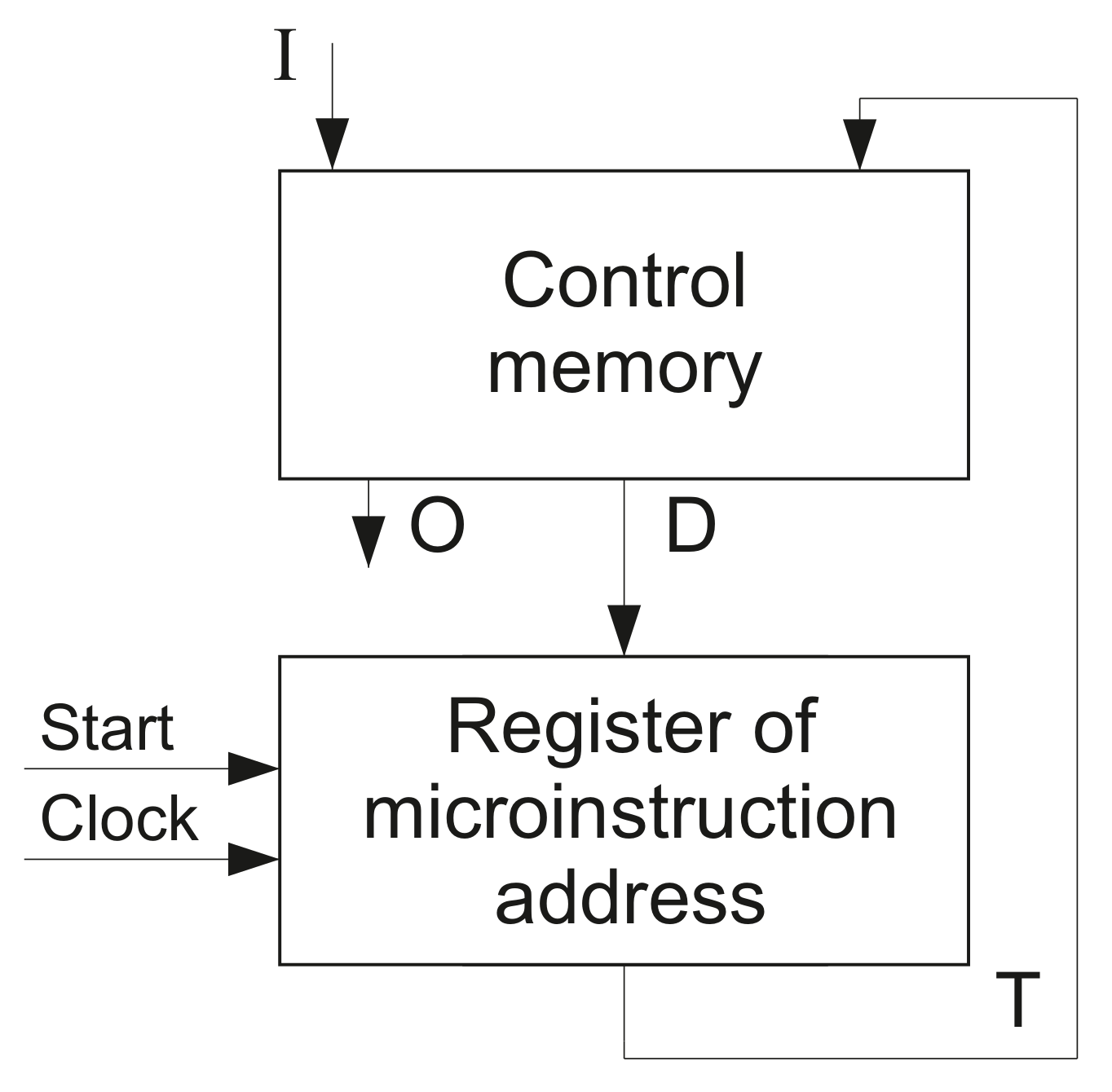
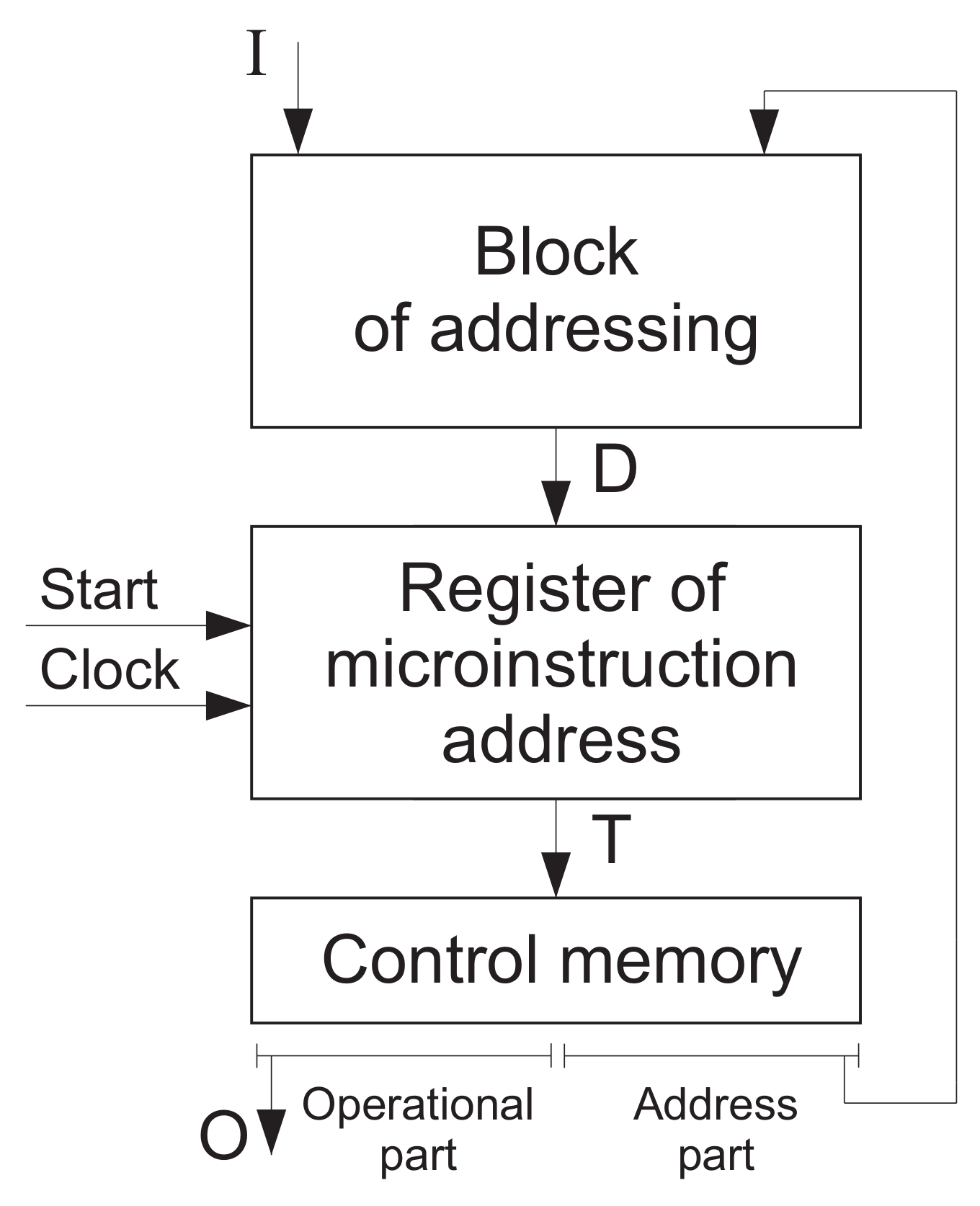
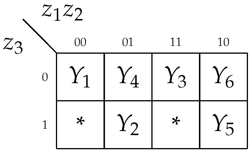
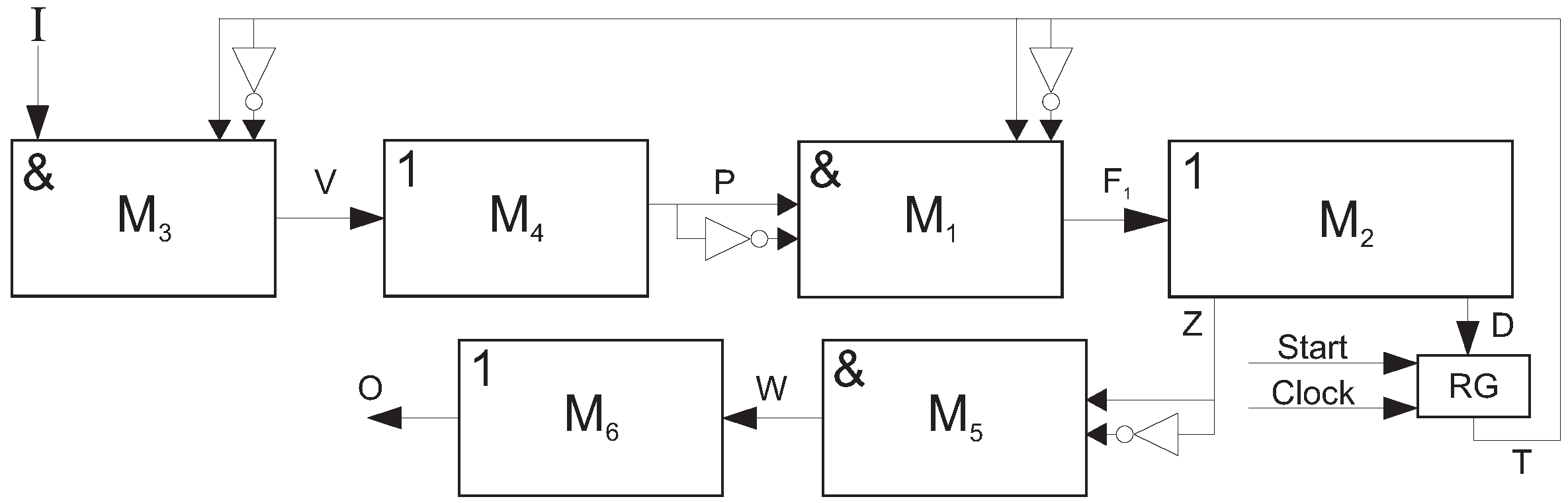
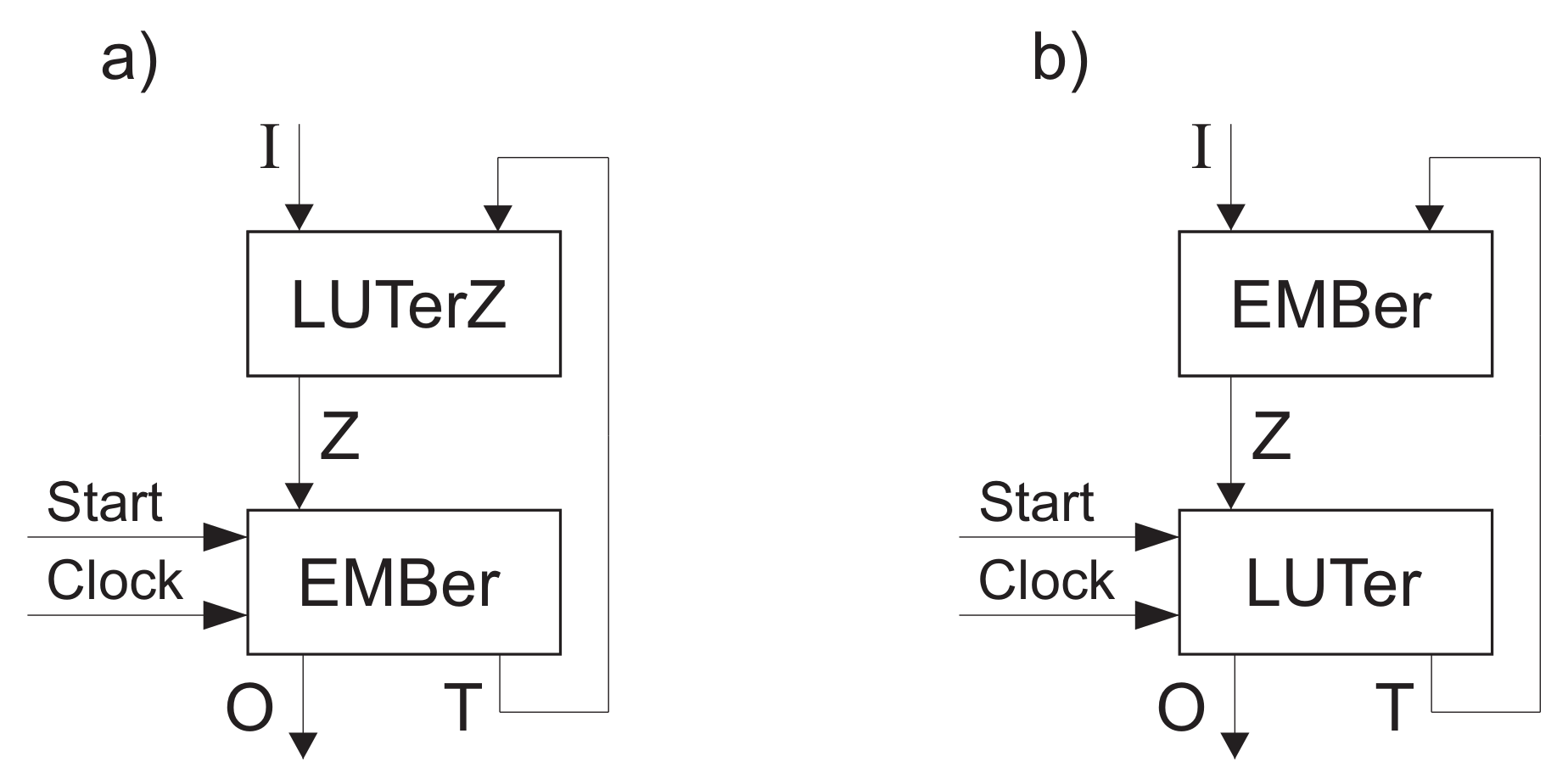
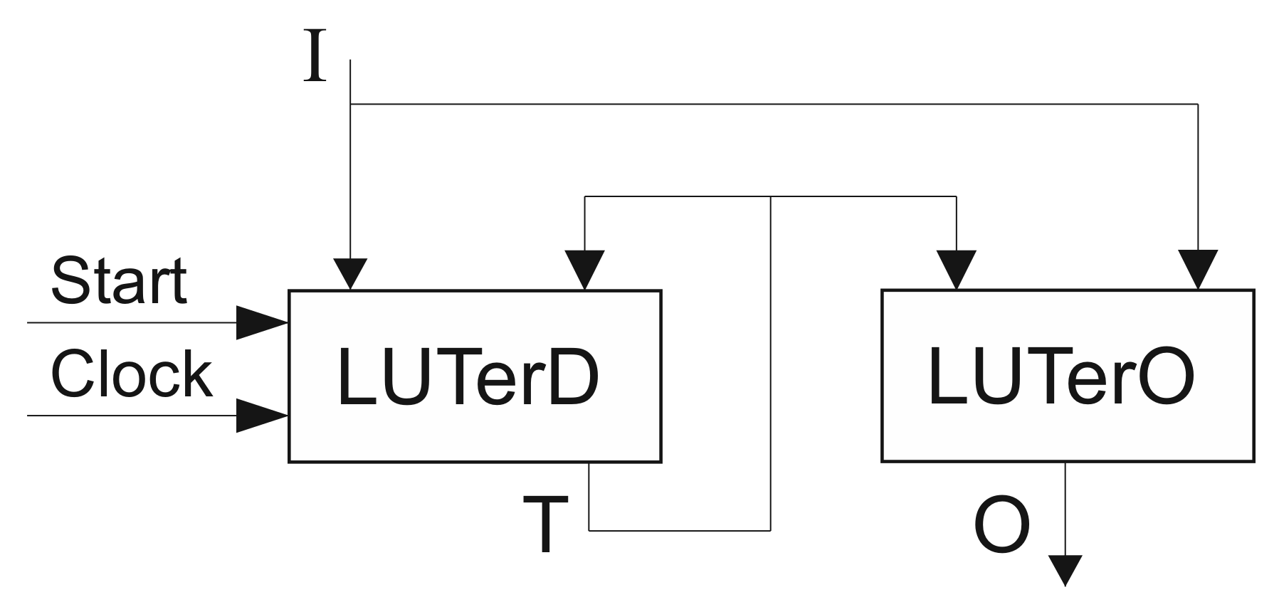
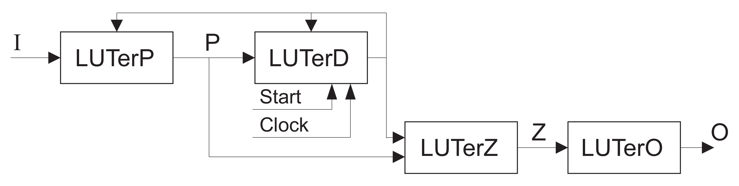
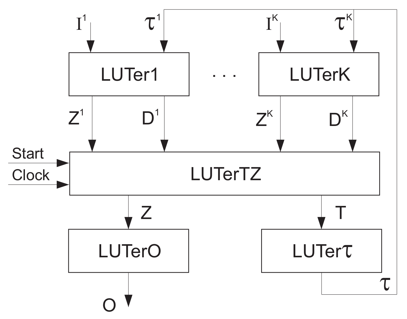
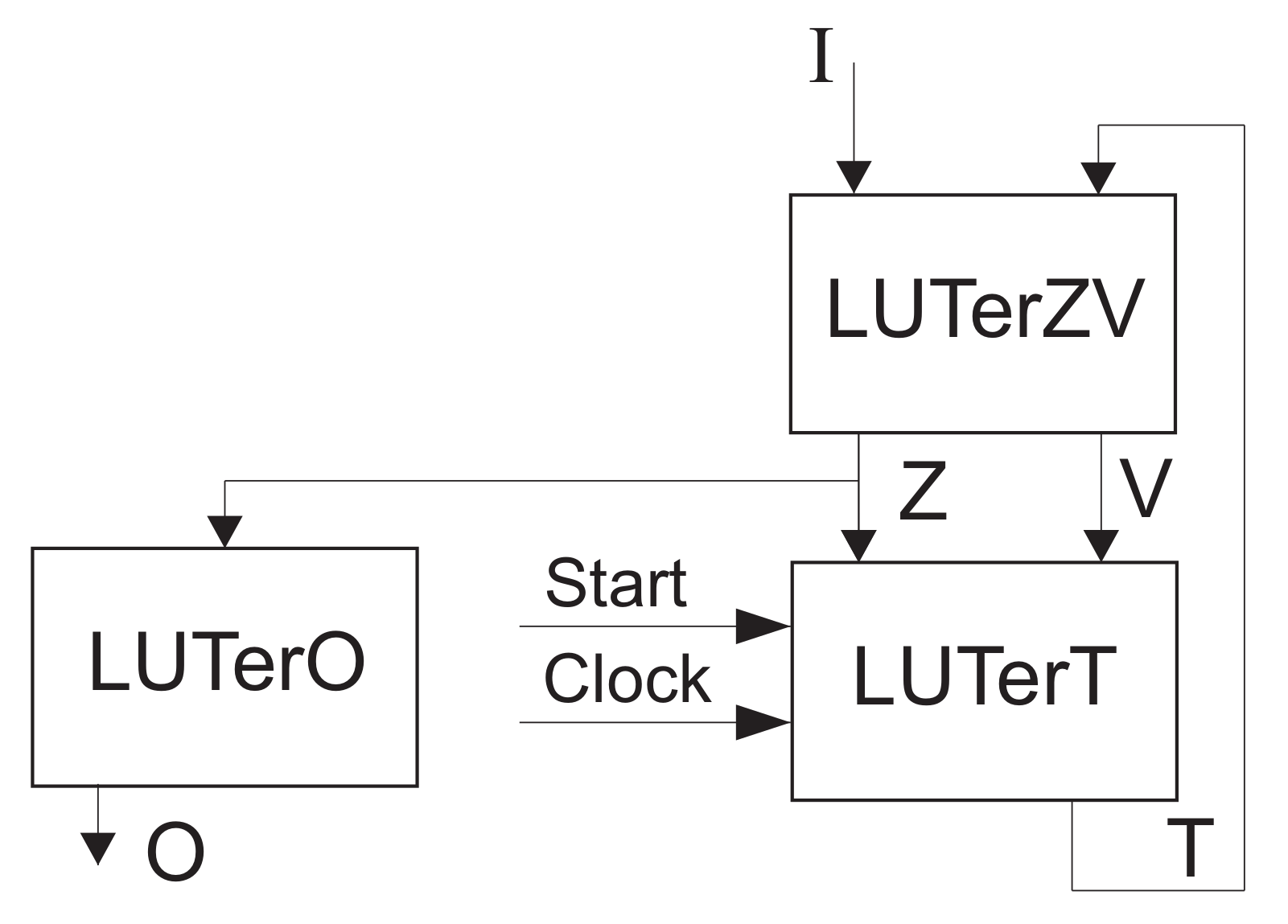
Table 1.
State transition table (STT) of Mealy finite state machine (FSM) .
| h | ||||
|---|---|---|---|---|
| 1 | ||||
| 2 | ||||
| 3 | ||||
| 4 | ||||
| 5 | ||||
| 6 | ||||
| 7 | ||||
| 1 | 8 |
Table 2.
Direct structure table (DST) of Mealy FSM .
| h | |||||||
|---|---|---|---|---|---|---|---|
| 00 | 01 | 1 | |||||
| 10 | 2 | ||||||
| 11 | 3 | ||||||
| 01 | 10 | 4 | |||||
| 01 | 5 | ||||||
| 10 | 00 | - | 6 | ||||
| 11 | 7 | ||||||
| 11 | 01 | 1 | 8 |
Table 3.
Direct structure table (DST) of Mealy FSM .
| h | |||||||
|---|---|---|---|---|---|---|---|
| 000 | 001 | 1 | |||||
| 010 | 2 | ||||||
| 001 | 001 | 3 | |||||
| 010 | 4 | ||||||
| 100 | 5 | ||||||
| 010 | 100 | 6 | |||||
| 011 | 7 | ||||||
| 101 | 8 | ||||||
| 100 | 010 | 9 | |||||
| 000 | - | - | 10 | ||||
| 011 | 001 | 11 | |||||
| 001 | 12 | ||||||
| 100 | 13 | ||||||
| 101 | 000 | 1 | - | - | 14 |
Table 4.
Table of replacement of P Mealy FSM .
| - | - | |||||
| - | - | |||||
| 000 | 001 | 010 | 100 | 011 | 101 |
Table 5.
DST of Mealy FSM .
| h | |||||||
|---|---|---|---|---|---|---|---|
| 000 | 001 | 1 | |||||
| 010 | 2 | ||||||
| 001 | 001 | 3 | |||||
| 010 | 4 | ||||||
| 100 | 5 | ||||||
| 010 | 100 | 6 | |||||
| 011 | 7 | ||||||
| 101 | 8 | ||||||
| 100 | 010 | 9 | |||||
| 000 | - | - | 10 | ||||
| 011 | 001 | 11 | |||||
| 001 | 12 | ||||||
| 100 | 13 | ||||||
| 101 | 000 | 1 | - | - | 14 |
Table 6.
DST of Mealy FSM .
| h | |||||||
|---|---|---|---|---|---|---|---|
| 000 | 001 | 1 | |||||
| 010 | 2 | ||||||
| 001 | 001 | 3 | |||||
| 010 | 4 | ||||||
| 100 | 5 | ||||||
| 010 | 100 | 6 | |||||
| 011 | 7 | ||||||
| 101 | 8 | ||||||
| 100 | 010 | 9 | |||||
| 000 | - | - | 10 | ||||
| 011 | 001 | 11 | |||||
| 001 | 12 | ||||||
| 100 | 13 | ||||||
| 101 | 000 | 1 | - | - | 14 |
Table 7.
DST of Mealy FSM .
| h | ||||||
|---|---|---|---|---|---|---|
| 000 | 0000 | - | 1 | |||
| 0001 | 2 | |||||
| 001 | 0010 | 3 | ||||
| 0011 | 4 | |||||
| 0100 | 5 | |||||
| 010 | 0101 | 6 | ||||
| 0110 | 7 | |||||
| 0111 | 8 | |||||
| 100 | 1000 | 9 | ||||
| 1001 | 10 | |||||
| 011 | 1010 | 11 | ||||
| 1011 | 12 | |||||
| 1100 | 13 | |||||
| 101 | 1 | 1101 | 14 |
Table 8.
Contents of programmable read-only memories (PROMs) of Mealy FSM .
| h | ||||||||||
|---|---|---|---|---|---|---|---|---|---|---|
| 0000 | 1 | 1 | 0 | 0 | 0 | 0 | 0 | 1 | 1 | |
| 0001 | 0 | 0 | 1 | 0 | 0 | 0 | 1 | 0 | 2 | |
| 0010 | 0 | 1 | 0 | 1 | 0 | 0 | 0 | 1 | 3 | |
| 0011 | 1 | 1 | 0 | 0 | 0 | 0 | 1 | 0 | 4 | |
| 0100 | 0 | 0 | 0 | 0 | 1 | 1 | 0 | 0 | 5 | |
| 0101 | 0 | 0 | 1 | 0 | 0 | 1 | 0 | 0 | 6 | |
| 0110 | 0 | 0 | 1 | 0 | 1 | 0 | 1 | 1 | 7 | |
| 0111 | 1 | 1 | 0 | 0 | 0 | 1 | 0 | 1 | 8 | |
| 1000 | 0 | 1 | 0 | 1 | 0 | 0 | 1 | 0 | 9 | |
| 1001 | 0 | 0 | 0 | 0 | 0 | 0 | 0 | 0 | 10 | |
| 1010 | 0 | 0 | 1 | 0 | 0 | 0 | 0 | 1 | 11 | |
| 1011 | 1 | 1 | 0 | 0 | 0 | 0 | 0 | 1 | 12 | |
| 1100 | 0 | 0 | 1 | 0 | 1 | 1 | 0 | 0 | 13 | |
| 1101 | 0 | 0 | 0 | 0 | 0 | 0 | 0 | 0 | 14 |
Table 9.
Part of truth table for FSM .
| Address | Contents of Cells | q | h | ||||||||||
|---|---|---|---|---|---|---|---|---|---|---|---|---|---|
| 0 | 1 | 0 | 0 | 0 | 0 | 0 | 0 | 0 | 1 | 0 | 1 | 9 | 5 |
| 0 | 1 | 0 | 0 | 1 | 1 | 1 | 0 | 0 | 0 | 1 | 0 | 10 | 4 |
| 0 | 1 | 0 | 1 | 0 | 0 | 0 | 0 | 0 | 1 | 0 | 1 | 11 | 5 |
| 0 | 1 | 0 | 1 | 1 | 1 | 1 | 0 | 0 | 0 | 1 | 0 | 12 | 4 |
| 0 | 1 | 1 | 0 | 0 | 0 | 0 | 0 | 0 | 1 | 0 | 1 | 13 | 5 |
| 0 | 1 | 1 | 0 | 1 | 1 | 1 | 0 | 0 | 0 | 1 | 0 | 14 | 4 |
| 0 | 1 | 1 | 1 | 0 | 0 | 0 | 0 | 0 | 1 | 0 | 1 | 15 | 5 |
| 0 | 1 | 1 | 1 | 1 | 1 | 1 | 0 | 0 | 0 | 1 | 0 | 16 | 4 |
Table 10.
Characteristics of Mealy FSM benchmarks.
| Benchmark | L | N | H | ||
|---|---|---|---|---|---|
| Category 0 | |||||
| bbtas | 2 | 2 | 6 | 9/4 | 24 |
| dk17 | 2 | 3 | 6 | 16/4 | 32 |
| dk27 | 1 | 2 | 5 | 10/4 | 14 |
| dk512 | 1 | 3 | 6 | 24/5 | 15 |
| ex3 | 2 | 2 | 6 | 14/4 | 36 |
| ex5 | 2 | 2 | 6 | 16/4 | 32 |
| lion | 2 | 1 | 5 | 5/3 | 11 |
| lion9 | 2 | 1 | 6 | 11/4 | 25 |
| mc | 3 | 5 | 6 | 8/3 | 10 |
| modulo12 | 1 | 1 | 5 | 12/4 | 24 |
| shiftreg | 1 | 1 | 5 | 16/4 | 16 |
| Category 1 | |||||
| bbara | 4 | 2 | 8 | 12/4 | 60 |
| bbsse | 7 | 7 | 12 | 26/5 | 56 |
| beecount | 3 | 4 | 7 | 10/4 | 28 |
| cse | 7 | 7 | 12 | 32/5 | 91 |
| dk14 | 3 | 5 | 8 | 26/5 | 56 |
| dk15 | 3 | 5 | 8 | 17/5 | 32 |
| dk16 | 2 | 3 | 9 | 75/7 | 108 |
| donfile | 2 | 1 | 7 | 24/5 | 96 |
| ex2 | 2 | 2 | 7 | 25/5 | 72 |
| ex4 | 6 | 9 | 11 | 18/5 | 21 |
| ex6 | 5 | 8 | 9 | 14/4 | 34 |
| ex7 | 2 | 2 | 12 | 17/5 | 36 |
| keyb | 7 | 7 | 12 | 22/5 | 170 |
| mark1 | 5 | 16 | 10 | 22/5 | 22 |
| opus | 5 | 6 | 10 | 18/5 | 22 |
| s27 | 4 | 1 | 8 | 11/4 | 34 |
| s386 | 7 | 7 | 12 | 23/5 | 64 |
| s8 | 4 | 1 | 8 | 15/4 | 20 |
| sse | 7 | 7 | 12 | 26/5 | 56 |
| Categories 2–4 | |||||
| ex1 | 9 | 19 | 16 | 80/7 | 138 |
| kirkman | 12 | 6 | 18 | 48/6 | 370 |
| planet | 7 | 19 | 14 | 86/7 | 115 |
| planet1 | 7 | 19 | 14 | 86/7 | 115 |
| pma | 8 | 8 | 14 | 49/6 | 73 |
| s1 | 8 | 7 | 14 | 54/6 | 106 |
| s1488 | 8 | 19 | 15 | 112/7 | 251 |
| s1494 | 8 | 19 | 15 | 118/7 | 250 |
| s1a | 8 | 6 | 15 | 86/7 | 107 |
| s208 | 11 | 2 | 17 | 37/6 | 153 |
| styr | 9 | 10 | 16 | 67/7 | 166 |
| tma | 7 | 9 | 13 | 63/6 | 44 |
| sand | 11 | 9 | 18 | 88/7 | 184 |
| s420 | 19 | 2 | 27 | 137/8 | 137 |
| s510 | 19 | 7 | 27 | 172/8 | 77 |
| s820 | 18 | 19 | 25 | 78/7 | 232 |
| s832 | 18 | 19 | 25 | 76/7 | 245 |
Table 11.
Experimental results for Mealy FSMs [123] (LUT counts).
Table 11.
Experimental results for Mealy FSMs [123] (LUT counts).
| Benchmark | Auto | One-Hot | JEDI | DEMAIN | |
|---|---|---|---|---|---|
| Category 0 | |||||
| bbtas | 5 | 5 | 5 | 5 | 8 |
| dk17 | 5 | 12 | 5 | 6 | 8 |
| dk27 | 3 | 5 | 4 | 4 | 7 |
| dk512 | 10 | 10 | 9 | 10 | 12 |
| ex3 | 9 | 9 | 9 | 9 | 11 |
| ex5 | 9 | 9 | 9 | 9 | 10 |
| lion | 2 | 5 | 2 | 2 | 6 |
| lion9 | 6 | 11 | 5 | 5 | 8 |
| mc | 4 | 7 | 4 | 5 | 6 |
| modulo12 | 7 | 7 | 7 | 7 | 9 |
| shiftreg | 2 | 6 | 2 | 2 | 4 |
| Category 1 | |||||
| bbara | 17 | 17 | 10 | 9 | 10 |
| bbsse | 33 | 37 | 24 | 26 | 26 |
| beecount | 19 | 19 | 14 | 16 | 14 |
| cse | 40 | 66 | 36 | 38 | 33 |
| dk14 | 10 | 27 | 10 | 12 | 12 |
| dk15 | 5 | 16 | 5 | 6 | 6 |
| dk16 | 15 | 34 | 12 | 14 | 11 |
| donfile | 31 | 31 | 22 | 26 | 21 |
| ex2 | 9 | 9 | 8 | 9 | 8 |
| ex4 | 15 | 13 | 12 | 13 | 11 |
| ex6 | 24 | 36 | 22 | 23 | 21 |
| ex7 | 4 | 5 | 4 | 4 | 6 |
| keyb | 43 | 61 | 40 | 42 | 37 |
| mark1 | 23 | 23 | 20 | 21 | 19 |
| opus | 28 | 28 | 22 | 26 | 21 |
| s27 | 6 | 18 | 6 | 6 | 6 |
| s386 | 26 | 39 | 22 | 25 | 20 |
| s8 | 9 | 9 | 9 | 9 | 9 |
| sse | 33 | 37 | 30 | 32 | 26 |
| Categories 2–4 | |||||
| ex1 | 70 | 74 | 53 | 57 | 40 |
| kirkman | 42 | 58 | 39 | 41 | 33 |
| planet | 131 | 131 | 88 | 94 | 78 |
| planet1 | 131 | 131 | 88 | 94 | 78 |
| pma | 94 | 94 | 86 | 91 | 72 |
| s1 | 65 | 99 | 61 | 64 | 54 |
| s1488 | 124 | 131 | 108 | 112 | 89 |
| s1494 | 126 | 132 | 110 | 117 | 90 |
| s1a | 49 | 81 | 43 | 54 | 38 |
| s208 | 12 | 31 | 10 | 11 | 9 |
| styr | 93 | 120 | 81 | 88 | 70 |
| tma | 45 | 39 | 39 | 41 | 30 |
| sand | 132 | 132 | 114 | 121 | 99 |
| s420 | 10 | 31 | 9 | 10 | 8 |
| s510 | 48 | 48 | 32 | 39 | 22 |
| s820 | 88 | 82 | 68 | 76 | 52 |
| s832 | 80 | 79 | 62 | 70 | 50 |
| Total | 1792 | 2104 | 1480 | 1601 | 1321 |
| Percentage | 135.65% | 159.27% | 112.04% | 121.20% | 100% |
Table 12.
Experimental results for Mealy FSMs [123] (the operating frequency, MHz).
Table 12.
Experimental results for Mealy FSMs [123] (the operating frequency, MHz).
| Benchmark | Auto | One-Hot | JEDI | DEMAIN | |
|---|---|---|---|---|---|
| Category 0 | |||||
| bbtas | 204.16 | 204.16 | 206.12 | 208.32 | 194.43 |
| dk17 | 199.28 | 167.00 | 199.39 | 172.19 | 147.22 |
| dk27 | 206.02 | 201.90 | 204.18 | 205.10 | 181.73 |
| dk512 | 196.27 | 196.27 | 199.75 | 197.49 | 175.63 |
| ex3 | 194.86 | 194.86 | 195.76 | 193.43 | 174.44 |
| ex5 | 180.25 | 180.25 | 181.16 | 181.76 | 162.56 |
| lion | 202.43 | 204.00 | 202.35 | 201.32 | 185.74 |
| lion9 | 205.30 | 185.22 | 206.38 | 205.86 | 167.28 |
| mc | 196.66 | 195.47 | 196.87 | 192.53 | 178.02 |
| modulo12 | 207.00 | 207.00 | 207.13 | 207.37 | 189.7 |
| shiftreg | 262.67 | 263.57 | 276.26 | 276.14 | 248.79 |
| Category 1 | |||||
| bbara | 193.39 | 193.39 | 212.21 | 198.46 | 183.32 |
| bbsse | 157.06 | 169.12 | 182.34 | 178.91 | 159.24 |
| beecount | 166.61 | 166.61 | 187.32 | 184.21 | 156.72 |
| cse | 146.43 | 163.64 | 178.12 | 174.19 | 153.24 |
| dk14 | 191.64 | 172.65 | 193.85 | 187.32 | 162.78 |
| dk15 | 192.53 | 185.36 | 194.87 | 188.54 | 175.42 |
| dk16 | 169.72 | 174.79 | 197.13 | 189.83 | 164.16 |
| donfile | 184.03 | 184.00 | 203.65 | 194.83 | 174.28 |
| ex2 | 198.57 | 198.57 | 200.14 | 199.75 | 188.95 |
| ex4 | 180.96 | 177.71 | 192.83 | 178.14 | 168.39 |
| ex6 | 169.57 | 163.80 | 176.59 | 174.12 | 156.42 |
| ex7 | 200.04 | 200.84 | 200.60 | 200.32 | 191.43 |
| keyb | 156.45 | 143.47 | 168.43 | 157.16 | 136.49 |
| mark1 | 162.39 | 162.39 | 176.18 | 169.65 | 153.48 |
| opus | 166.20 | 166.20 | 178.32 | 168.79 | 157.42 |
| s27 | 198.73 | 191.50 | 199.13 | 198.43 | 185.15 |
| s386 | 168.15 | 173.46 | 179.15 | 169.21 | 164.65 |
| s8 | 180.02 | 178.95 | 181.23 | 180.39 | 168.32 |
| sse | 157.06 | 169.12 | 174.63 | 169.69 | 158.14 |
| Categories 2–4 | |||||
| ex1 | 150.94 | 139.76 | 176.87 | 186.14 | 164.32 |
| kirkman | 141.38 | 154.00 | 156.68 | 143.76 | 155.36 |
| planet | 132.71 | 132.71 | 187.14 | 185.73 | 174.68 |
| planet1 | 132.71 | 132.71 | 187.14 | 185.73 | 173.29 |
| pma | 146.18 | 146.18 | 169.83 | 153.57 | 156.12 |
| s1 | 146.41 | 135.85 | 157.16 | 149.17 | 145.32 |
| s1488 | 138.50 | 131.94 | 157.18 | 153.12 | 141.27 |
| s1494 | 149.39 | 145.75 | 164.34 | 159.42 | 155.63 |
| s1a | 153.37 | 176.40 | 169.17 | 158.12 | 166.36 |
| s208 | 174.34 | 176.46 | 178.76 | 172.87 | 166.42 |
| styr | 137.61 | 129.92 | 145.64 | 138.83 | 118.02 |
| tma | 163.88 | 147.80 | 164.14 | 168.19 | 137.48 |
| sand | 115.97 | 115.97 | 126.82 | 120.63 | 120.07 |
| s420 | 173.88 | 176.46 | 177.25 | 172.87 | 186.35 |
| s510 | 177.65 | 177.65 | 198.32 | 183.18 | 199.05 |
| s820 | 152.00 | 153.16 | 176.58 | 166.29 | 175.69 |
| s832 | 145.71 | 153.23 | 173.78 | 160.03 | 174.39 |
| Total | 8127.08 | 8061.22 | 8718.87 | 8461.10 | 7917.10 |
| Percentage | 102.65% | 101.82% | 110.13% | 106.87% | 100% |
Table 13.
Experimental results [122] (LUT counts).
Table 13.
Experimental results [122] (LUT counts).
| Benchmark | P | [122] | ||
|---|---|---|---|---|
| ex1 | 22 | 19 | 48 | 36 |
| kirkman | 30 | 26 | 27 | 11 |
| planet | 21 | 16 | 51 | 38 |
| planet1 | 21 | 16 | 51 | 38 |
| pma | 28 | 23 | 27 | 14 |
| s1 | 26 | 23 | 24 | 12 |
| s1488 | 24 | 21 | 52 | 37 |
| s1494 | 28 | 24 | 50 | 39 |
| s208 | 29 | 23 | 8 | 7 |
| s420 | 38 | 36 | 8 | 7 |
| s510 | 39 | 36 | 22 | 15 |
| s820 | 40 | 34 | 47 | 36 |
| s832 | 41 | 34 | 47 | 35 |
| sand | 27 | 23 | 29 | 16 |
| styr | 26 | 20 | 31 | 18 |
| Total | 440 | 374 | 522 | 359 |
| Percentage | 123% | 104% | 145% | 100% |
Table 14.
Experimental results [122] (the operating frequency, MHz).
Table 14.
Experimental results [122] (the operating frequency, MHz).
| Benchmark | P | [122] | ||
|---|---|---|---|---|
| ex1 | 141.43 | 105.78 | 158.28 | 212.93 |
| kirkman | 125.78 | 107.81 | 155.11 | 174.73 |
| planet | 122.01 | 105.41 | 124.31 | 187.95 |
| planet1 | 122.01 | 105.41 | 124.31 | 187.95 |
| pma | 115.41 | 114.49 | 127.65 | 186.22 |
| s1 | 124.49 | 117.80 | 132.85 | 178.84 |
| s1488 | 127.80 | 112.79 | 131.77 | 186.37 |
| s1494 | 122.79 | 124.92 | 135.73 | 181.62 |
| s208 | 144.92 | 128.04 | 144.05 | 209.36 |
| s420 | 148.04 | 112.66 | 152.65 | 192.14 |
| s510 | 122.66 | 111.42 | 138.75 | 192.87 |
| s820 | 121.42 | 88.65 | 133.36 | 163.18 |
| s832 | 98.65 | 115.57 | 100.53 | 184.69 |
| sand | 135.57 | 104.68 | 146.78 | 178.65 |
| styr | 114.68 | 116.47 | 115.69 | 181.22 |
| Total | 1887.66 | 1671.90 | 2021.82 | 2798.72 |
| Percentage | 67.4% | 59.7% | 72.2% | 100% |
Table 15.
Experimental results [122] (the consumed power, Watts).
Table 15.
Experimental results [122] (the consumed power, Watts).
| Benchmark | P | [122] | ||
|---|---|---|---|---|
| ex1 | 3.560 | 3.290 | 3.014 | 2.918 |
| kirkman | 4.922 | 3.562 | 2.811 | 2.476 |
| planet | 3.222 | 3.756 | 1.727 | 1.527 |
| planet1 | 3.222 | 3.756 | 1.727 | 1.527 |
| pma | 4.778 | 4.915 | 4.257 | 3.683 |
| s1 | 3.694 | 3.813 | 3.578 | 3.058 |
| s1488 | 1.586 | 2.412 | 1.449 | 1.785 |
| s1494 | 1.730 | 2.398 | 1.453 | 1.302 |
| s208 | 3.005 | 3.544 | 2.574 | 2.248 |
| s420 | 1.604 | 3.384 | 1.543 | 1.292 |
| s510 | 1.883 | 1.996 | 1.878 | 1.682 |
| s820 | 2.465 | 2.161 | 1.756 | 1.843 |
| s832 | 2.515 | 2.504 | 2.193 | 1.732 |
| sand | 2.579 | 2.578 | 2.385 | 2.017 |
| styr | 1.467 | 1.556 | 1.307 | 1.112 |
| Total | 42.232 | 45.625 | 33.652 | 30.202 |
| Percentage | 139.8% | 151% | 111.4% | 100% |
Table 16.
Experimental results [132] (LUT counts).
Table 16.
Experimental results [132] (LUT counts).
| Benchmark | Auto | One-Hot | JEDI | ||
|---|---|---|---|---|---|
| Category 0 | |||||
| bbtas | 5 | 5 | 5 | 8 | 9 |
| dk17 | 5 | 12 | 5 | 8 | 10 |
| dk27 | 3 | 5 | 4 | 7 | 9 |
| dk512 | 10 | 10 | 9 | 12 | 14 |
| ex3 | 9 | 9 | 9 | 11 | 14 |
| ex5 | 9 | 9 | 9 | 10 | 12 |
| lion | 2 | 5 | 2 | 6 | 8 |
| lion9 | 6 | 11 | 5 | 8 | 10 |
| mc | 4 | 7 | 4 | 6 | 8 |
| modulo12 | 7 | 7 | 7 | 9 | 11 |
| shiftreg | 2 | 6 | 2 | 4 | 6 |
| Category 1 | |||||
| bbara | 17 | 17 | 10 | 10 | 14 |
| bbsse | 33 | 37 | 24 | 26 | 29 |
| beecount | 19 | 19 | 14 | 14 | 16 |
| cse | 40 | 66 | 36 | 33 | 35 |
| dk14 | 16 | 27 | 10 | 12 | 14 |
| dk15 | 15 | 16 | 12 | 8 | 11 |
| dk16 | 15 | 34 | 12 | 11 | 13 |
| donfile | 31 | 31 | 24 | 21 | 24 |
| ex2 | 9 | 9 | 8 | 8 | 10 |
| ex4 | 15 | 13 | 12 | 11 | 13 |
| ex6 | 24 | 36 | 22 | 21 | 23 |
| ex7 | 4 | 5 | 4 | 6 | 8 |
| keyb | 43 | 61 | 40 | 37 | 40 |
| mark1 | 23 | 23 | 20 | 19 | 21 |
| opus | 28 | 28 | 22 | 21 | 23 |
| s27 | 6 | 18 | 6 | 6 | 8 |
| s386 | 26 | 39 | 22 | 20 | 22 |
| s8 | 9 | 9 | 9 | 9 | 11 |
| sse | 33 | 37 | 30 | 26 | 29 |
| Categories 2–4 | |||||
| ex1 | 70 | 74 | 53 | 40 | 44 |
| kirkman | 42 | 58 | 39 | 33 | 35 |
| planet | 131 | 131 | 88 | 78 | 82 |
| planet1 | 131 | 131 | 88 | 78 | 82 |
| pma | 94 | 94 | 86 | 72 | 76 |
| s1 | 65 | 99 | 61 | 54 | 58 |
| s1488 | 124 | 131 | 108 | 89 | 93 |
| s1494 | 126 | 132 | 110 | 90 | 94 |
| s1a | 49 | 81 | 43 | 38 | 42 |
| s208 | 12 | 31 | 10 | 9 | 11 |
| styr | 93 | 120 | 81 | 70 | 78 |
| tma | 45 | 39 | 39 | 30 | 34 |
| sand | 132 | 132 | 114 | 99 | 103 |
| s420 | 10 | 31 | 9 | 8 | 10 |
| s510 | 48 | 48 | 32 | 22 | 23 |
| s820 | 88 | 82 | 68 | 52 | 56 |
| s832 | 80 | 79 | 62 | 50 | 52 |
| Total | 1808 | 2104 | 1489 | 1320 | 1448 |
| Percentage | 124.86% | 145.30% | 102.83% | 91.16% | 100% |
Table 17.
Experimental results [132] (the maximum operating frequency, MHz).
Table 17.
Experimental results [132] (the maximum operating frequency, MHz).
| Benchmark | Auto | One-Hot | JEDI | ||
|---|---|---|---|---|---|
| Category 0 | |||||
| bbtas | 204.16 | 204.16 | 206.12 | 194.43 | 201.47 |
| dk17 | 199.28 | 167.00 | 199.39 | 147.22 | 172.99 |
| dk27 | 206.02 | 201.90 | 204.18 | 181.73 | 190.32 |
| dk512 | 196.27 | 196.27 | 199.75 | 175.63 | 187.45 |
| ex3 | 194.86 | 194.86 | 195.76 | 174.44 | 187.26 |
| ex5 | 180.25 | 180.25 | 181.16 | 162.56 | 162.56 |
| lion | 202.43 | 204.00 | 202.35 | 185.74 | 195.73 |
| lion9 | 205.30 | 185.22 | 206.38 | 167.28 | 183.45 |
| mc | 196.66 | 195.47 | 196.87 | 178.02 | 182.95 |
| modulo12 | 207.00 | 207.00 | 207.13 | 189.70 | 201.74 |
| shiftreg | 262.67 | 263.57 | 276.26 | 248.79 | 253.72 |
| Category 1 | |||||
| bbara | 193.39 | 193.39 | 212.21 | 183.32 | 210.21 |
| bbsse | 157.06 | 169.12 | 182.34 | 159.24 | 193.43 |
| beecount | 166.61 | 166.61 | 187.32 | 156.72 | 194.47 |
| cse | 146.43 | 163.64 | 178.12 | 153.24 | 182.62 |
| dk14 | 191.64 | 172.65 | 193.85 | 162.78 | 201.39 |
| dk15 | 192.53 | 185.36 | 194.87 | 175.42 | 206.74 |
| dk16 | 169.72 | 174.79 | 197.13 | 164.16 | 199.14 |
| donfile | 184.03 | 184.00 | 203.65 | 174.28 | 206.83 |
| ex2 | 198.57 | 198.57 | 200.14 | 188.95 | 196.58 |
| ex4 | 180.96 | 177.71 | 192.83 | 168.39 | 196.18 |
| ex6 | 169.57 | 163.80 | 176.59 | 156.42 | 187.53 |
| ex7 | 200.04 | 200.84 | 200.60 | 191.43 | 204.16 |
| keyb | 156.45 | 143.47 | 168.43 | 136.49 | 178.59 |
| mark1 | 162.39 | 162.39 | 176.18 | 153.48 | 182.37 |
| opus | 166.20 | 166.20 | 178.32 | 157.42 | 186.34 |
| s27 | 198.73 | 191.50 | 199.13 | 185.15 | 201.26 |
| s386 | 168.15 | 173.46 | 179.15 | 164.65 | 192.34 |
| s8 | 180.02 | 178.95 | 181.23 | 168.32 | 191.32 |
| sse | 157.06 | 169.12 | 174.63 | 158.14 | 171.18 |
| Categories 2–4 | |||||
| ex1 | 150.94 | 139.76 | 176.87 | 164.32 | 180.72 |
| kirkman | 141.38 | 154.00 | 156.68 | 155.36 | 184.62 |
| planet | 132.71 | 132.71 | 187.14 | 174.68 | 212.45 |
| planet1 | 132.71 | 132.71 | 187.14 | 173.29 | 212.45 |
| pma | 146.18 | 146.18 | 169.83 | 156.12 | 192.43 |
| s1 | 146.41 | 135.85 | 157.16 | 145.32 | 145.32 |
| s1488 | 138.50 | 131.94 | 157.18 | 141.27 | 182.14 |
| s1494 | 149.39 | 145.75 | 164.34 | 155.63 | 186.49 |
| s1a | 153.37 | 176.40 | 169.17 | 166.36 | 188.92 |
| s208 | 174.34 | 176.46 | 178.76 | 166.42 | 192.15 |
| styr | 137.61 | 129.92 | 145.64 | 118.02 | 164.52 |
| tma | 163.88 | 147.80 | 164.14 | 137.48 | 182.72 |
| sand | 115.97 | 115.97 | 126.82 | 120.07 | |
| s420 | 173.88 | 176.46 | 177.25 | 186.35 | 218.62 |
| s510 | 177.65 | 177.65 | 198.32 | 199.05 | 221.19 |
| s820 | 152.00 | 153.16 | 176.58 | 175.69 | 195.73 |
| s832 | 145.71 | 153.23 | 173.78 | 174.39 | 199.18 |
| Total | 8127.08 | 8061.22 | 8718.87 | 7873.36 | 9005.11 |
| Percentage | 90.25% | 89.52% | 96.82% | 87.43% | 100% |
Table 18.
Experimental results [132] (area-time products, LUTs ).
Table 18.
Experimental results [132] (area-time products, LUTs ).
| Benchmark | Auto | One-Hot | JEDI | ||
|---|---|---|---|---|---|
| Category 0 | |||||
| bbtas | 24.49 | 24.49 | 24.26 | 41.15 | 44.67 |
| dk17 | 25.09 | 71.86 | 25.08 | 54.34 | 57.81 |
| dk27 | 14.56 | 24.76 | 19.59 | 38.52 | 47.29 |
| dk512 | 50.95 | 50.95 | 45.06 | 68.33 | 74.69 |
| ex3 | 46.19 | 46.19 | 45.97 | 63.06 | 74.76 |
| ex5 | 49.93 | 49.93 | 49.68 | 61.52 | 73.82 |
| lion | 9.88 | 24.51 | 9.88 | 32.30 | 40.87 |
| lion9 | 29.23 | 59.39 | 24.23 | 47.82 | 54.51 |
| mc | 20.34 | 35.81 | 20.32 | 33.70 | 43.73 |
| modulo12 | 33.82 | 33.82 | 33.80 | 47.44 | 54.53 |
| shiftreg | 7.61 | 22.76 | 7.24 | 16.08 | 23.65 |
| Category 1 | |||||
| bbara | 87.91 | 87.91 | 47.12 | 54.55 | 66.60 |
| bbsse | 210.11 | 218.78 | 131.62 | 163.28 | 149.93 |
| beecount | 114.04 | 114.04 | 74.74 | 89.33 | 82.27 |
| cse | 273.17 | 403.32 | 202.11 | 215.35 | 191.65 |
| dk14 | 83.49 | 156.39 | 51.59 | 73.72 | 69.52 |
| dk15 | 77.91 | 86.32 | 61.58 | 45.60 | 53.21 |
| dk16 | 88.38 | 194.52 | 60.87 | 67.01 | 65.28 |
| donfile | 168.45 | 168.48 | 117.85 | 120.50 | 116.04 |
| ex2 | 45.32 | 45.32 | 39.97 | 42.34 | 50.87 |
| ex4 | 82.89 | 73.15 | 62.23 | 65.32 | 66.27 |
| ex6 | 141.53 | 219.78 | 124.58 | 134.25 | 122.65 |
| ex7 | 20.00 | 24.90 | 19.94 | 31.34 | 39.18 |
| keyb | 274.85 | 425.18 | 237.49 | 271.08 | 223.98 |
| mark1 | 141.63 | 141.63 | 113.52 | 123.79 | 115.15 |
| opus | 168.47 | 168.47 | 123.37 | 133.40 | 123.43 |
| s27 | 30.19 | 93.99 | 30.13 | 32.41 | 39.75 |
| s386 | 154.62 | 224.84 | 122.80 | 121.47 | 114.38 |
| s8 | 49.99 | 50.29 | 49.66 | 53.47 | 57.50 |
| sse | 210.11 | 218.78 | 171.79 | 164.41 | 169.41 |
| Categories 2–4 | |||||
| ex1 | 463.76 | 529.48 | 299.66 | 243.43 | 243.47 |
| kirkman | 297.07 | 376.62 | 248.91 | 212.41 | 189.58 |
| planet | 987.11 | 987.11 | 470.24 | 446.53 | 385.97 |
| planet1 | 987.11 | 987.11 | 470.24 | 450.11 | 385.97 |
| pma | 643.04 | 643.04 | 506.39 | 461.18 | 394.95 |
| s1 | 443.96 | 728.74 | 388.14 | 371.59 | 399.12 |
| s1488 | 895.31 | 992.88 | 687.11 | 630.00 | 510.60 |
| s1494 | 843.43 | 905.66 | 669.34 | 578.29 | 504.05 |
| s1a | 319.49 | 459.18 | 254.18 | 228.42 | 222.32 |
| s208 | 68.83 | 175.68 | 55.94 | 54.08 | 57.25 |
| styr | 675.82 | 923.65 | 556.17 | 593.12 | 474.11 |
| tma | 274.59 | 263.87 | 237.60 | 218.21 | 186.08 |
| sand | 1138.23 | 1138.23 | 898.91 | 824.52 | 719.58 |
| s420 | 57.51 | 175.68 | 50.78 | 42.93 | 45.74 |
| s510 | 270.19 | 270.19 | 161.36 | 110.52 | 103.98 |
| s820 | 578.95 | 535.39 | 385.09 | 295.98 | 286.11 |
| s832 | 549.04 | 515.56 | 356.77 | 286.71 | 261.07 |
| Total | 12228.61 | 14168.64 | 8844.90 | 8554.93 | 7877.31 |
| Percentage | 155.24% | 179.87% | 112.28% | 108.60% | 100% |
Publisher’s Note: MDPI stays neutral with regard to jurisdictional claims in published maps and institutional affiliations. |
© 2021 by the authors. Licensee MDPI, Basel, Switzerland. This article is an open access article distributed under the terms and conditions of the Creative Commons Attribution (CC BY) license (https://creativecommons.org/licenses/by/4.0/).
Share and Cite
MDPI and ACS Style
Barkalov, A.; Titarenko, L.; Krzywicki, K. Structural Decomposition in FSM Design: Roots, Evolution, Current State—A Review. Electronics 2021, 10, 1174. https://0-doi-org.brum.beds.ac.uk/10.3390/electronics10101174
AMA Style
Barkalov A, Titarenko L, Krzywicki K. Structural Decomposition in FSM Design: Roots, Evolution, Current State—A Review. Electronics. 2021; 10(10):1174. https://0-doi-org.brum.beds.ac.uk/10.3390/electronics10101174
Chicago/Turabian StyleBarkalov, Alexander, Larysa Titarenko, and Kazimierz Krzywicki. 2021. "Structural Decomposition in FSM Design: Roots, Evolution, Current State—A Review" Electronics 10, no. 10: 1174. https://0-doi-org.brum.beds.ac.uk/10.3390/electronics10101174
Note that from the first issue of 2016, this journal uses article numbers instead of page numbers. See further details here.