LTPS TFTs with an Amorphous Silicon Buffer Layer and Source/Drain Extension
by

Hye In Kim
1, 
Jung Min Sung
2,
Hyung Uk Cho
2,
Yong Jo Kim
2,
Young Gwan Park
2 and
Woo Young Choi
1,* 1
Department of Electronics Engineering, Sogang University, Seoul 04107, Korea
2
CAE Team, Display R&D Center, Samsung Display, Gyeonggi-do 17113, Korea
*
Author to whom correspondence should be addressed.
Electronics 2021, 10(1), 29; https://0-doi-org.brum.beds.ac.uk/10.3390/electronics10010029
Submission received: 18 November 2020
/
Revised: 21 December 2020
/
Accepted: 23 December 2020
/
Published: 28 December 2020
(This article belongs to the Special Issue Reliability Assessment and Modeling of Optical and Semiconductor Devices)
Abstract
:A low leakage poly-Si thin film transistor (TFT) is proposed featuring hydrogenated amorphous silicon (a-Si:H) buffer layer and source/drain extension (SDE) by using technology computer aided design (TCAD) simulation. This architecture reduces off-current effectively by suppressing two leakage current generation mechanisms with little on-current loss. The amorphous silicon buffer layer having large bandgap energy (Eg) suppresses both thermal generation and minimum leakage current, which leads to higher on/off current ratio. In addition, the formation of lightly doped region near the drain alleviates the field-enhanced generation in the off-state by reducing electric field. TCAD simulation results show that the proposed TFT shows more than three orders of magnitude lower off-current than low-temperature polycrystalline silicon (LTPS) TFTs, while maintaining on-current.
1. Introduction
A low-temperature polycrystalline silicon thin-film transistor (LTPS TFT) fabricated on a glass substrate has been considered as one of the most attractive options for active-matrix organic light emitting diode (AMOLED) display applications because it has higher electron mobility and driving current than an amorphous-silicon (a-Si) TFT and oxide TFT [1,2,3,4,5,6,7]. However, there are critical disadvantages of LTPS TFTs: low on/off current ratio and high leakage current [8,9,10,11,12,13,14,15,16,17]. For the improvement of display quality, the leakage current of TFTs which act as pixel switches should be minimized [1,2,3,4,5,6]. The main leakage mechanism of LTPS TFTs is the generation-recombination (G-R) occurring at the drain-side depletion region [6,7,8,9]. The G-R is classified into the two sub-mechanisms [9,10,11,12,13]. One is the thermal generation depending on trap density, energy bandgap, and temperature while being independent of gate voltage (VG). It is dominant under the low electric field condition, especially near the flat band voltage. Thus, it determines minimum leakage current. The other is the field-enhanced generation including field-enhanced thermal emission (Poole–Frenkel), phonon-assisted tunneling, trap-assisted tunneling, and band-to-band tunneling (BTBT). It strongly depends on VG and trap density because the tunneling barrier narrows with increasing VG and trap density. Under the high electric field condition, the field-enhanced generation makes the leakage current independent of temperature and exponentially dependent on VG [1,11].
Several methods have already been proposed for lower leakage current and higher performance [18,19,20,21,22,23,24,25,26,27,28,29,30] including field-induced drain (FID) [28,29] and current and electric field split (CES) design TFTs [30]. However, both FID and CES design TFTs suffer from complex fabrication process and large parasitic capacitance because they need one more field plate.
In this paper, we propose the LTPS TFTs using an amorphous silicon buffer layer and source/drain extension (SDE) which lowers leakage current by suppressing both thermal generation and field-enhanced generation in the off-state. The hydrogenated a-Si (a-Si:H) layer whose bandgap energy (Eg) is 1.8 eV is located between the active layer and gate insulator to suppress thermal generation. The SDE reduces the electric field at the channel/drain junction, which alleviates field-enhanced generation. It should be noted that the introduction of an amorphous silicon buffer layer and SDE causes only little on-state current loss. It is because the amorphous silicon layer is very thin (<4 nm) [25,26,27], because the defects and crystallinity of the amorphous silicon layer can be optimized by controlling the silane (SiH4) and hydrogen (H2) gas flow rates [26] and because the current is spread to the entire SDE region [14,15,16]. Thus, without serious on-current loss, the on/off current ratio becomes >103 × higher in high VD. Additionally, in terms of process flow, sidewall spacer and implant-to-silicide (ITS) techniques can be introduced [31,32].
2. Proposed Process Flow
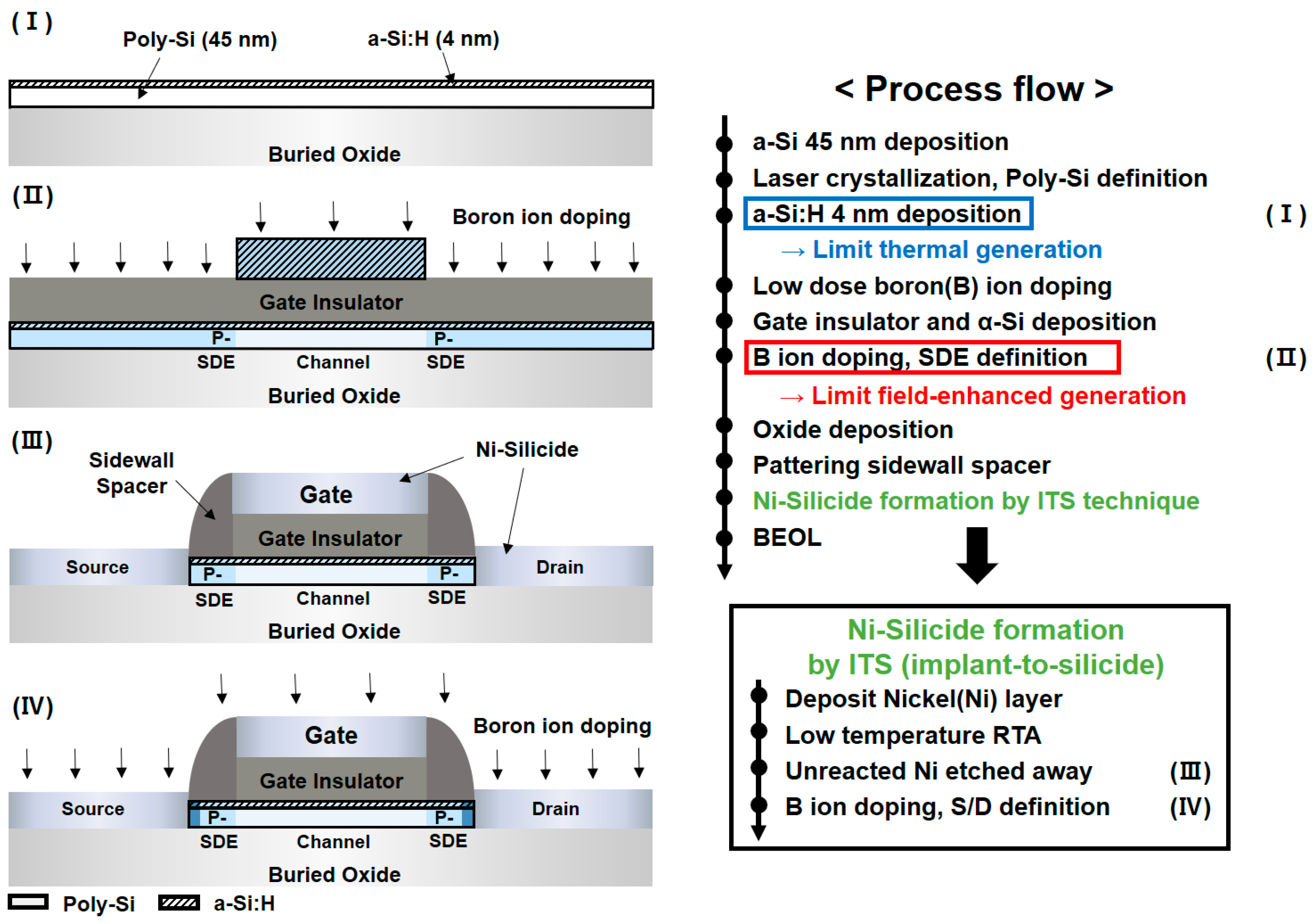
Figure 1 shows the key fabrication steps of our proposed LTPS TFT. First, a 45 nm thick a-Si layer is deposited and then crystallized by excimer laser annealing (ELA) to convert a-Si into poly-Si. On the poly-Si layer, a 4 nm thick amorphous silicon buffer layer is deposited controlling the ratio of silane (SiH4) to hydrogen (H2) [26]. In addition, to make 4 nm amorphous silicon, it is necessary to keep the temperature and radio frequency (RF) power low to prevent crystallization for plasma enhanced chemical vapor deposition (PECVD) [25,26]. Then, SiO2 and a-Si layers are deposited. The a-Si layer is patterned to form the gate electrode layer. Subsequently, an oxide layer is deposited and anisotropically etched to form a sidewall spacer around the gate. The most important process step is Ni silicide formation. For self-aligned silicidation to form the silicided S/D, the deposition of a thin Ni layer is followed by the low temperature annealing (500 °C, 40 s) process [31,32]. Next, the unreacted Ni layer is removed and the ITS process is performed to form S/D. Implanted dopants are diffused out of silicide at the channel–S/D interface.
3. Device Structure and Simulation Methodology
To investigate the proposed device, a two-carrier and two-dimensional device simulation was performed by using a technology computer-aided design (TCAD) simulator [33]. The Poisson equation, continuity equation, and physics models including charge transports were used to calculate electrostatic potential, carrier flow, and G-R. The Shockley–Read–Hall (SRH) recombination and Hurkx BTBT model considering trap-assisted tunneling, phonon-assisted tunneling, and BTBT were also used.
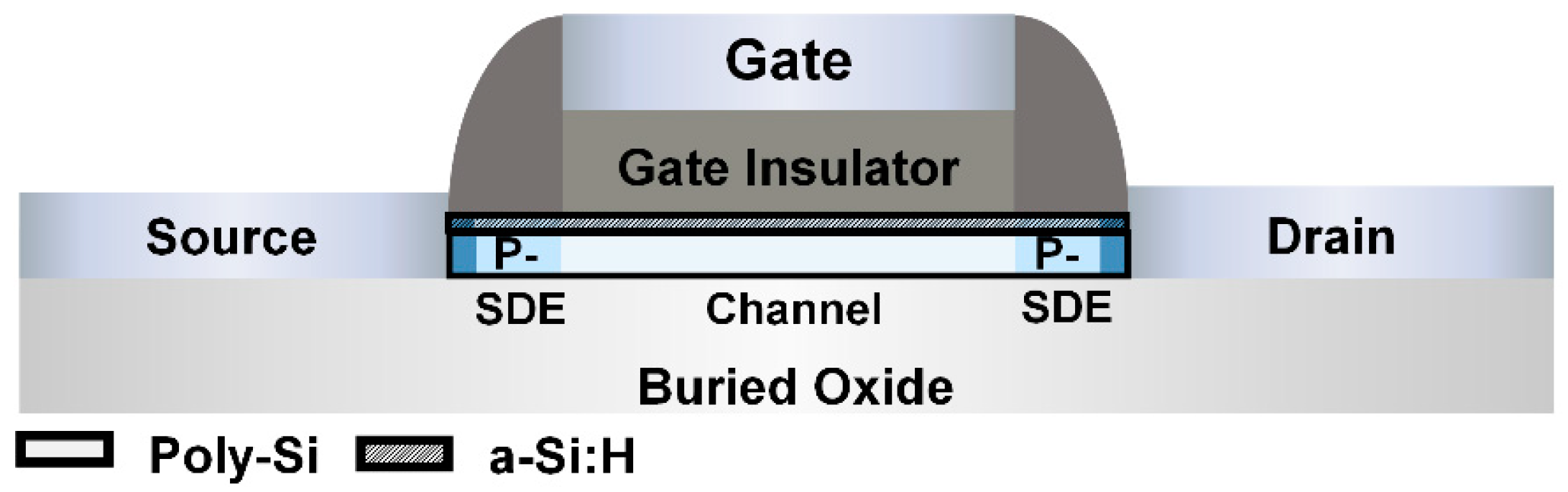
Figure 2 shows the device structure of the proposed p-type LTPS TFT with a 0.75 μm long SDE and 4 nm thick amorphous silicon buffer layer. Uniform doping profiles are assumed in the poly-Si and amorphous silicon layer. Boron doping concentration at the channel, source/drain, and SDE are 12.3 × 1016 cm−3, 1.64 × 1019 cm−3, and 4.6 × 1017 cm−3, respectively. The thicknesses of the active layer (tact) and the gate insulator (tGI) are 0.045 and 0.12 μm, respectively. The channel width (W) and length (L) are 3.5 and 4 μm, respectively. Device dimensions and doping profiles refer to the literature [15,21]. In addition, 10 nm long highly-doped regions are located between the SDE and silicide region considering dopant segregation whose doping concentration is the same as that of the source/drain region of conventional LTPS TFTs [34]. Detailed device parameters are summarized in Table 1.
The subgap density of states (DOSs) of LTPS and amorphous silicon are assumed to be uniformly distributed throughout the poly-Si and amorphous silicon [35,36,37]. Additionally, the capture cross section for traps is assumed to be 10−12 cm2 in the simulation. The detailed subgap DOS N (E) equation is derived by using the superposition of the exponential tail-level and Gaussian deep-level states as:
where the N (E) is DOS, E is energy level, EC is the conduction band minimum, EV is the valence band maximum, W is the width of the energy distribution, and EG is the energy of the center of the trap distribution. The subscript A and D mean the acceptor-like and the donor-like DOS, respectively. The subscript T and G mean the tail and the Gaussian distribution, respectively. The detailed DOS parameters of poly-Si and amorphous silicon are summarized in Table 2.
4. Simulation Results and Discussion
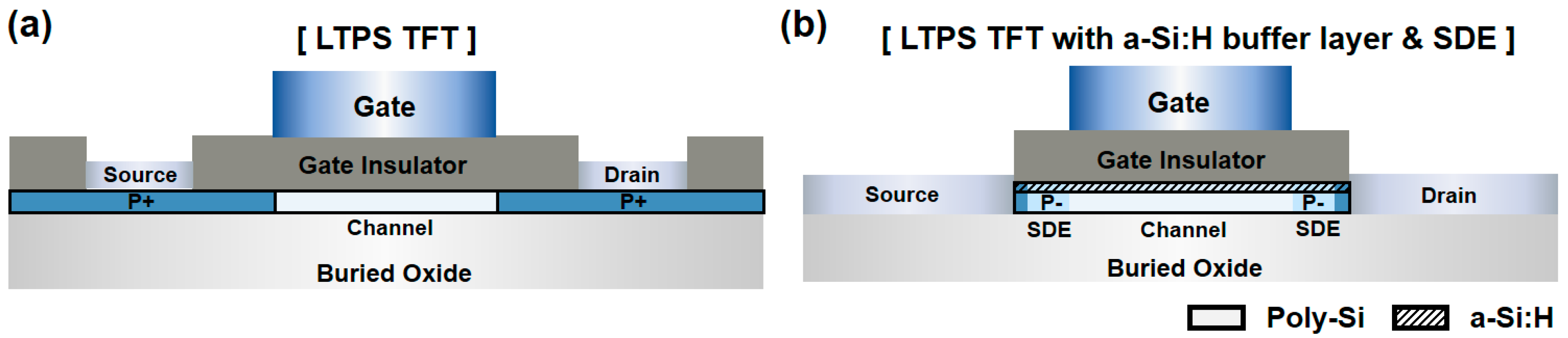
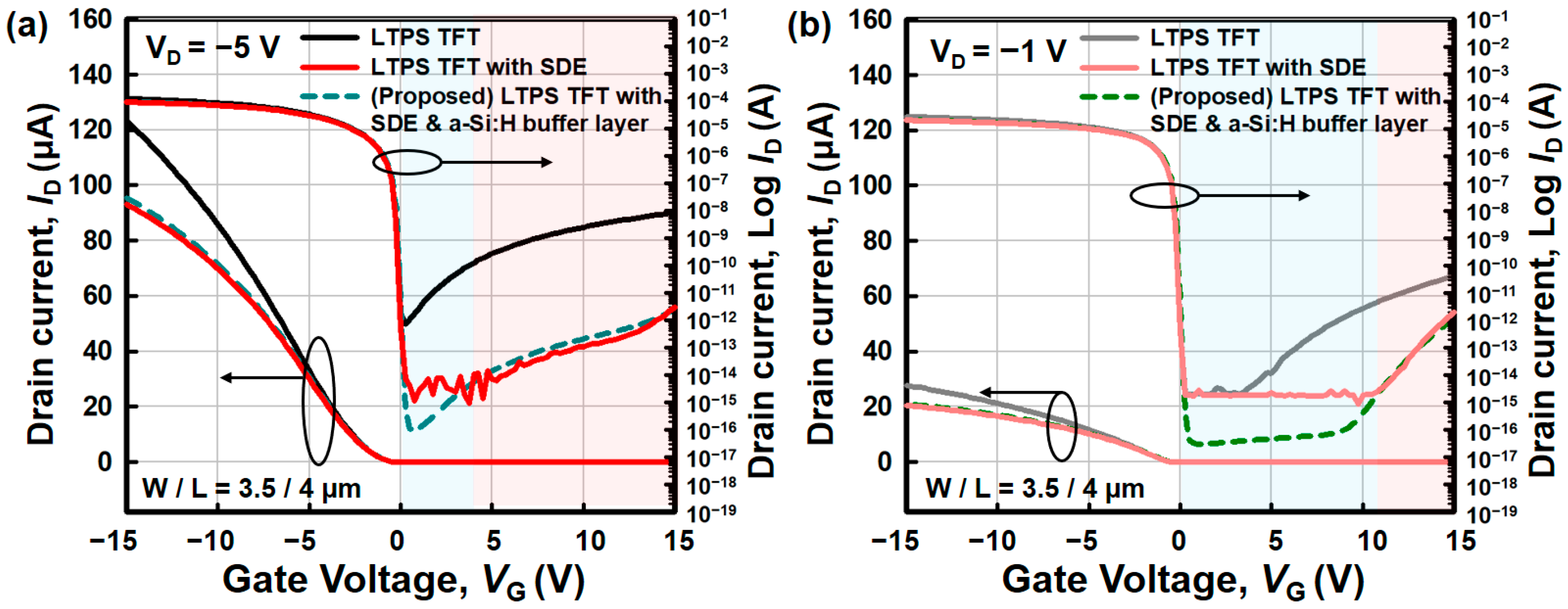
Figure 3 shows the two simulated structures of the LTPS TFTs with and without 4 nm thick amorphous silicon buffer layer and 0.75 µm long SDE: conventional and our proposed LTPS TFTs. Figure 4 shows the transfer curves of the structures. Our proposed LTPS TFT shows dramatical reduction of off-current with the help of the SDE and amorphous silicon buffer layer. According to the literature [18,19,20,21], SDE suppresses field-enhanced generation current under the high electric field condition while wide bandgap materials located between the gate insulator and channel reduces thermal generation current under the low electric field condition. Our proposed LTPS TFT not only reduces leakage current under the high electric field condition, but also lowers the minimum leakage current under low electric field condition with <7% on-current loss. Because both thermal and field-enhanced generation depend on temperature and electric field, they can be investigated separately.
The field effect mobility (μ) was calculated by the gm.max method and the threshold voltage (Vth) was observed at ID = 10−7 A by constant current method. The μ of TFTs is 73.9 cm2/V∙S (LTPS TFT) and 63.82 cm2/V∙S for proposed TFT, respectively. In addition, Vth is −0.48 V for LTPS TFT and −0.42 V for proposed TFT, respectively. It is observed that conventional LTPS TFT shows higher on-current than the rest of TFTs and that the LTPS TFTs with SDE show the same on-current as our proposed LTPS TFTs. Thus, on-current loss is originated from the SDE rather than an amorphous silicon layer. On the contrary, in the off-state, our proposed LTPS TFTs show the lowest leakage current because thermal generation is suppressed by the amorphous silicon layer. However, as VG increases, our proposed LTPS TFTs show almost the same leakage current as the LTPS TFTs with SDE because field-enhanced generation is dominant under the high electric field condition.
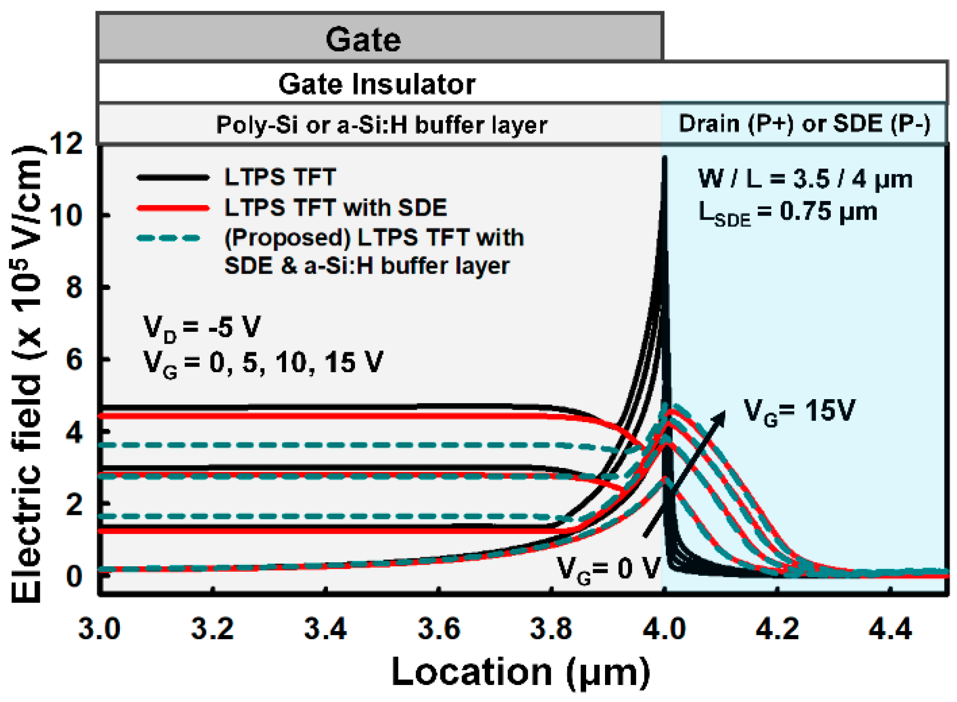
The main off-current component of LTPS TFTs tunneling is through traps at the near-drain grain boundaries [10,11,12,13] which becomes dominant when the electric field exceeds 0.7 MV/cm [11]. Figure 5 compares the electric field distribution of the three kinds of LTPS TFTs along the channel surface. VG varies from 0 to 15 V while drain voltage (VD) is fixed at −5 V. It is observed that the LTPS TFTs with SDE have analogous electric field distribution near the gate edge of the gate and that conventional LTPS TFTs show higher electric field peak than the rest of LTPS TFTs. The maximum electric field is ~1.2 MV/cm in the case of conventional LTPS TFTs and 0.5 MV/cm in the case of the rest of LTPS TFTs. From Figure 4 and Figure 5, it can be concluded that the SDE suppresses the field-enhanced tunneling current effectively.
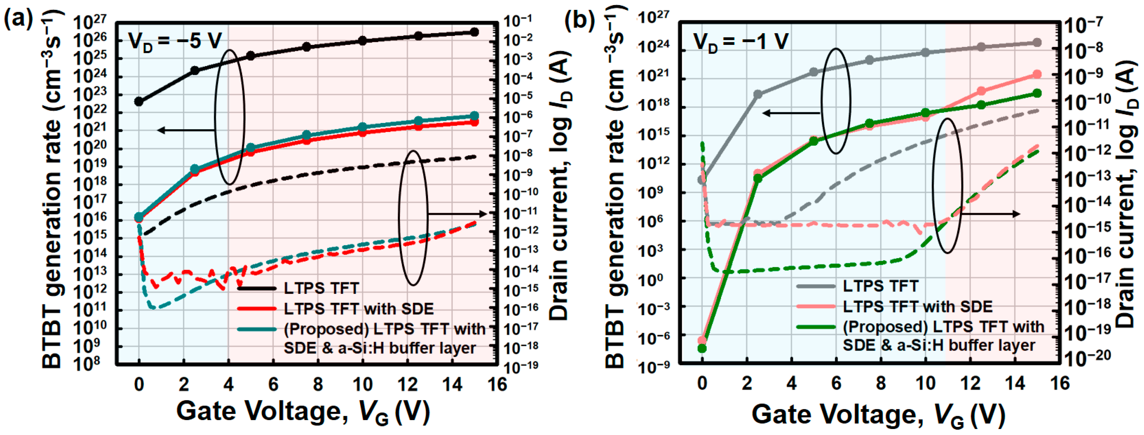
Figure 6 shows the BTBT generation rate including tunneling through traps at VD = −5 V and VD = −1 V. It is observed that drain current (ID) shows similar behavior to the BTBT generation rate as VG increases. It means that the major leakage current mechanism under the high electric field condition is the field-enhanced tunneling. In addition, it should be noted that conventional LTPS TFTs show a higher BTBT rate than the rest of LTPS TFTs and that our proposed LTPS TFTs show almost the same BTBT rate as the LTPS TFTs with SDE.
From the above shown simulation results, it can be concluded that under the high voltage condition, the SDE reduces the electric field and tunneling rate while an amorphous silicon layer rarely affects leakage current. It is clearly shown that the role of the SDE is the electric field and tunneling suppression under the high electric field condition. Even if the BTBT rate is lowered by the SDE, it is difficult to lower the minimum leakage current below 10−15 A. The LTPS TFTs with and without the SDE have no difference in minimum leakage under the low electric field condition, which means that the dominant mechanism at a low electric field is independent of electric field. The minimum leakage of the LTPS TFTs with SDE is almost the same as that of conventional ones at low VD. On the contrary, our proposed LTPS TFTs show lower minimum leakage current and higher on/off current ratio than the rest of LTPS TFTs. Thus, it can be concluded that minimum leakage current reduction is originated from the wide bandgap of the amorphous silicon layer.
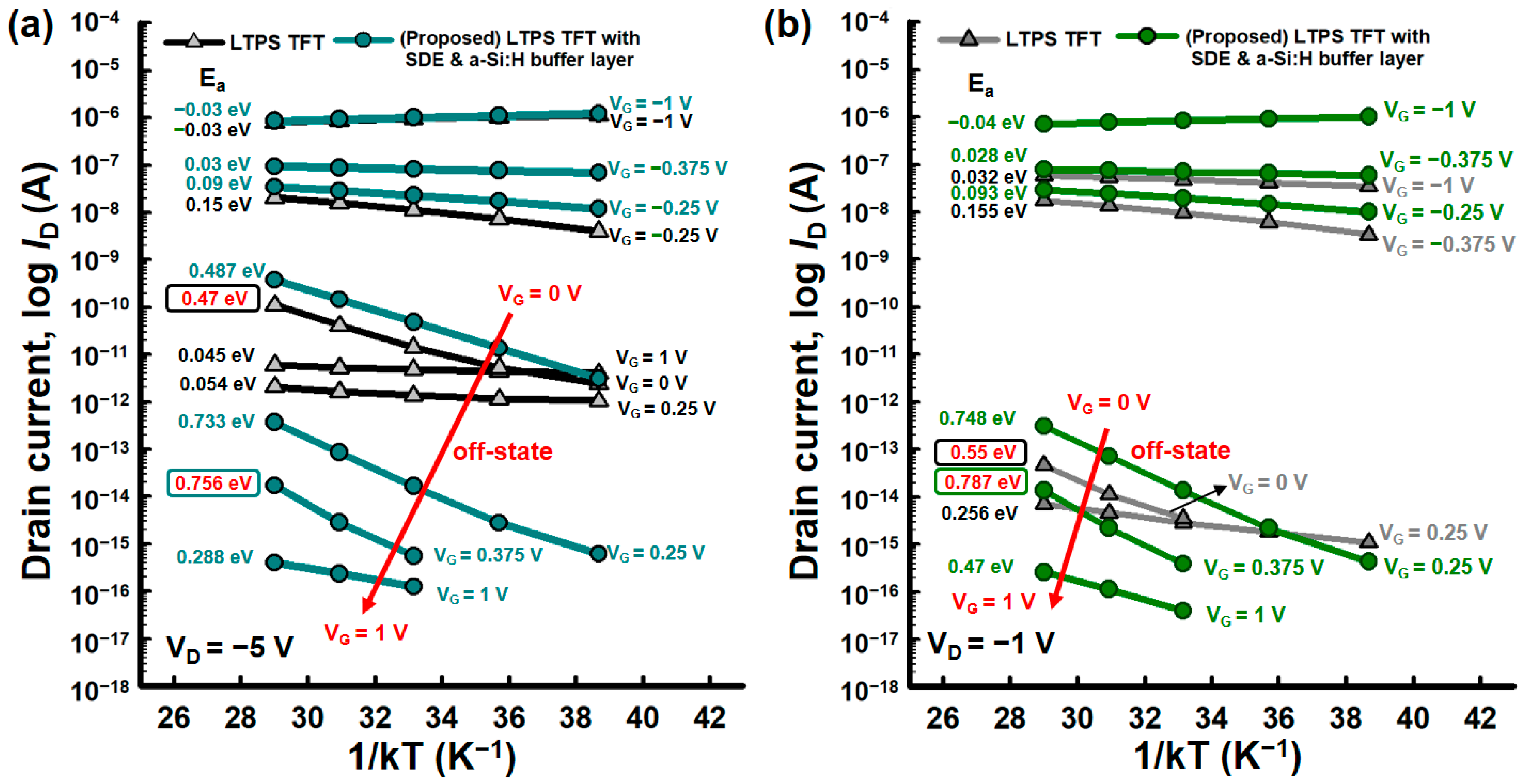
Off-current is a function of temperature and electrostatic potential barrier height. As VD and VG increase, the potential barrier felt by the carriers in traps decreases and trap levels approach the valence and conduction band. Thus, the field-enhanced generation becomes dominant under the high field condition. At low voltage, on the contrary, carriers in the midgap are expected to overcome ~Eg/2. Thus, thermal generation becomes more dominant than field-enhanced generation:
Activation energy (Ea) indicates the potential barrier height as shown below:
where k is Boltzmann constant and T is absolute temperature. The Ea is extracted as follows:
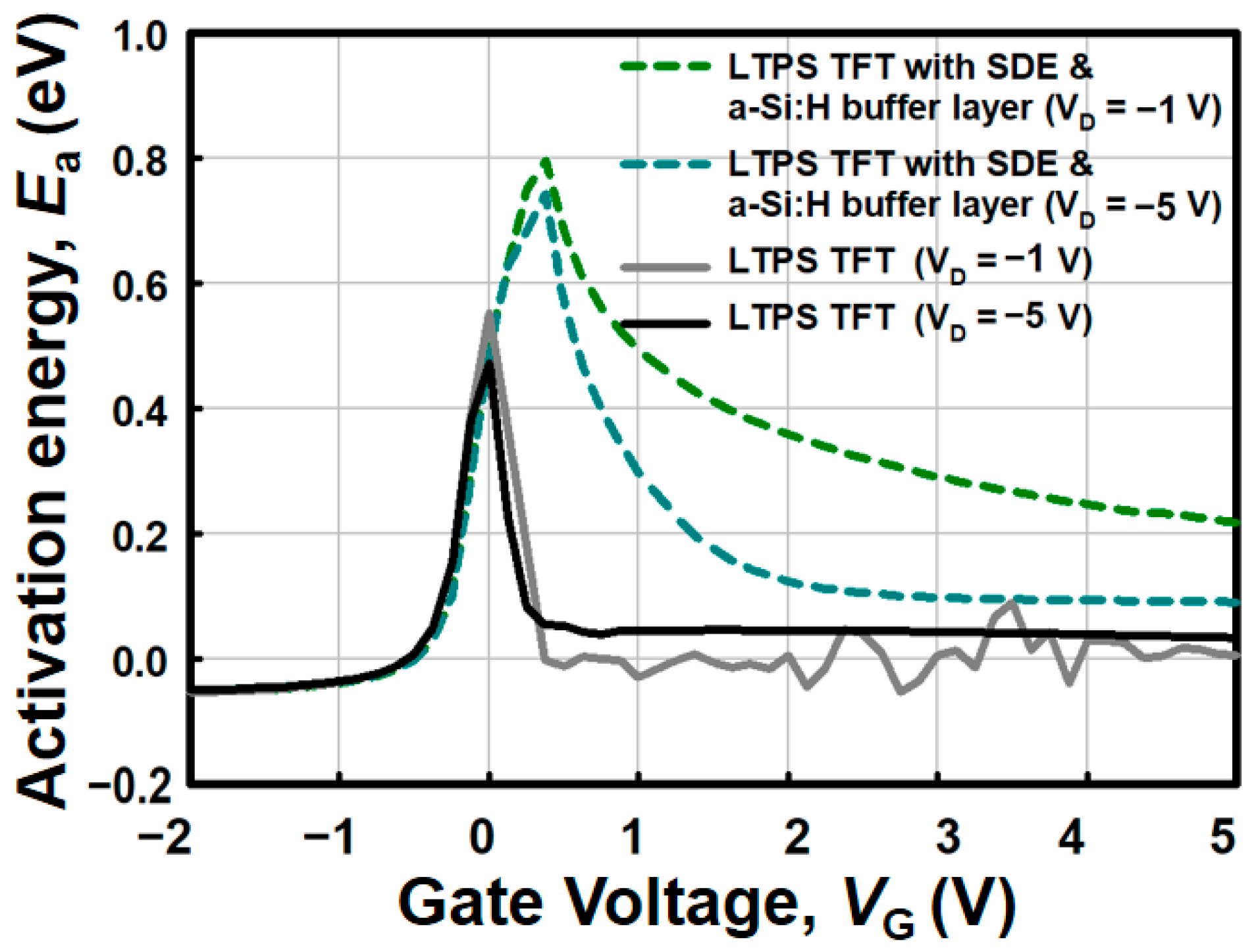
Figure 7 shows the Arrhenius plots of conventional and our proposed LTPS TFTs. It is observed that drain leakage current strongly depends on Ea as a function of VG. The Eas extracted from Figure 7 are shown as a function of VG in Figure 8 [13]. Ea depends strongly on VG and VD. At VD = −1 V, the maximum value of activation energy is ~0.55 eV in the case of conventional LTPS TFTs, which corresponds to the potential barrier height required for trap emission. Because Ea is ~Eg/2, thermal generation is a dominant leakage mechanism. In addition, in the case of our proposed LTPS TFTs, the Ea is ~0.8 eV at VG = 0.375 V, which is a typical value of amorphous silicon. Additionally, the proposed LTPS TFTs suppress thermal generation effectively by controlling Eg.
5. Conclusions
A novel LTPS TFT is proposed to reduce the off-state current by suppressing thermal generation and field-enhanced generation with the help of an amorphous silicon buffer layer and SDE. The deposition of the thin amorphous silicon buffer layer on the poly-Si active layer limits thermal generation and reduces the off-state minimum current by three orders of magnitude in high VD thanks to the increased Ea originated from the large Eg of amorphous silicon. In addition, the lightly doped region near the drain reduces the field-enhanced generation and provides sufficient separation gap between the channel and drain silicide.
Author Contributions
Writing–Original Draft & Data curation, H.I.K.; Formal analysis, H.I.K.; Data fitting & project management, J.M.S., H.U.C., Y.J.K. Y.G.P.; Writing–Review & Editing, W.Y.C.; Validation W.Y.C.; Supervision W.Y.C. All authors have read and agreed to the published version of the manuscript.
Funding
This research received no external funding.
Institutional Review Board Statement
Not applicable.
Informed Consent Statement
Not applicable.
Data Availability Statement
Data sharing not applicable.
Acknowledgments
This work was supported in part by Samsung Display, in part by the NRF of Korea funded by the MSIT under Grant NRF-2019M3F3A1A02072089 (Intelligent Semiconductor Technology Development Program), NRF-2018R1A2A2A05019651 (Mid-Career Researcher Program), NRF-2016M3A7B4909668 (Nano-Material Technology Development Program), in part by the IITP funded by the MSIT under Grant IITP-2020-2018-0-01421 (Information Technology Research Center Program), and in part by the MOTIE/KSRC under Grant 10080575 (Technology Innovation Program).
Conflicts of Interest
The authors declare no conflict of interest.
References
- Brotherton, S.D. Polycrystalline silicon thin film transistor. Semicond. Sci. Technol. 1995, 10, 721–738. [Google Scholar] [CrossRef]
- Serikawa, T.; Shirai, T.; Okamoto, A.; Suyama, S. Low Temperature Fabrication of High-Mobility Poly-Si TFT’s for Large-Area LCD’s. IEEE Trans. Electron Devices 1989, 36, 1929–1933. [Google Scholar] [CrossRef]
- Lih, J.J.; Sung, C.F.; Li, C.H.; Hsiao, T.H.; Lee, H.H. Comparison of a-Si and poly-Si for AMOLED displays. J. Soc. Inf. Disp. 2012, 12, 367–371. [Google Scholar] [CrossRef]
- Stewart, M.; Howell, R.S.; Pires, L.; Hatalis, M.K. Polysilicon TFT Technology for Active Matrix OLED Displays. IEEE Trans. Electron Devices 2001, 48, 845–851. [Google Scholar] [CrossRef]
- Wang, H.; Jiang, L.L.; Wang, N.; Yu, H.Y.; Lin, X.P. A Charge Storage Based Enhancement Mode AlGaN/GaN High Electron Mobility Transistor. Mater. Sci. Forum 2018, 913, 870–875. [Google Scholar] [CrossRef]
- Megherbi, M.L.; Pezzimenti, F.; Dehimi, L.; Saadoune, M.A.; Della Corte, F.G. Analysis of trapping effects on the forward current-voltage characteristics of al-implanted 4H-SiC p-i-n Diodes. IEEE Trans. Electron Devices 2018, 65, 3371–3378. [Google Scholar] [CrossRef]
- Pezzimenti, F. Modeling of the steady state and switching characteristics of a normally-off 4H-SiC trench bipolar-mode FET. IEEE Trans. Electron Devices 2013, 60, 1404–1411. [Google Scholar] [CrossRef]
- Anvarifard, M.K.; Orouji, A.A. Proper Electrostatic Modulation of Electric Field in a Reliable Nano-SOI with a Developed Channel. IEEE Trans. Electron Devices 2018, 65, 1653–1657. [Google Scholar] [CrossRef]
- Shirai, S.; Serikawa, T. Electrical Analysis of High-Mobility Poly-Si TFT’s Made from Laser-Irradiated Sputtered Si Films. IEEE Trans. Electron Devices 1922, 39, 450–452. [Google Scholar] [CrossRef]
- Fossum, J.G.; Ortiz-Conde, A.; Shichijo, H.; Banerjee, S.K. Anomalous Leakage Current in LPCVD Polysilicon MOSFET’s. IEEE Trans. Electron Devices 1985, 32, 1878–1884. [Google Scholar] [CrossRef]
- Brotherton, S.D.; Ayres, J.R.; Trainor, M.J. Control and analysis of leakage currents in poly-Si thin-film transistors. J. Appl. Phys. 1996, 79, 895. [Google Scholar] [CrossRef]
- Walker, P.M.; Uno, S.; Mizuta, H. Simulation Study of the Dependence of Submicron Polysilicon Thin-Film Transistor Output Characteristics on Grain Boundary Position. Jpn. J. Appl. Phys. 2005, 44, 8322–8328. [Google Scholar] [CrossRef] [Green Version]
- Park, J.; Jang, K.S.; Shin, D.G.; Shin, M.; Yi, J.S. Gate-induced drain leakage current characteristics of p-type polycrystalline silicon thin film transistors aged by off-state stress. Solid-State Electron. 2018, 148, 20–26. [Google Scholar] [CrossRef]
- Kim, C.H.; Sohn, K.S. Temperature dependent leakage currents in polycrystalline silicon thin film transistors. J. Appl. Phys. 1997, 81, 8084–8090. [Google Scholar] [CrossRef]
- Vincent, C.; Chantre, A.; Bois, D. Electric field effect on the thermal emission of traps in semiconductor junctions. J. Appl. Phys. 1979, 50, 5484–5487. [Google Scholar] [CrossRef]
- Martin, P.A.; Streetman, B.G.; Hess, K. Electric field enhanced emission from non-Coulombic traps in semiconductors. J. Appl. Phys. 1981, 52, 7409–7415. [Google Scholar] [CrossRef]
- Pecora, A.; Schillizzi, M.; Tallarida, G.; Fortunato, G.; Reita, C.; Migliorato, P. Off-Current in Polycrystalline Silicon Thin Film Transistors: An Analysis of the Thermally Generated Component. Solid-State Electron. 1995, 38, 845–850. [Google Scholar] [CrossRef]
- Kimura, M.; Taya, J.; Nakashima, A. Temperature Dependences of I-V Characteristics of SD and LDD Poly-Si TFTs. IEEE Electron Device Lett. 2012, 33, 682–684. [Google Scholar] [CrossRef]
- Kimura, M. Behavior Analysis of an LDD Poly-Si TFT Using 2-D Device Simulation. IEEE Trans. Electron Devices 2012, 59, 705–709. [Google Scholar] [CrossRef]
- Kimura, M.; Nakashima, A. Mechanism Analysis of Current-Voltage Characteristic in a Lightly Doped Drain Polycrystalline Silicon Thin-Film Transistor Using Activation Energy. Jpn. J. Appl. Phys. 2012, 51, 03CA05. [Google Scholar] [CrossRef]
- Nakashima, A.; Kimura, M. Mechanism Analysis of Off-Leakage Current in an LDD Poly-Si TFT Using Activation Energy. IEEE Electron Device Lett. 2011, 32, 764–766. [Google Scholar] [CrossRef]
- Orouji, A.A.; Kumar, M.J. Leakage Current Reduction Techniques in Poly-Si TFTs for Active Matrix Liquid Crystal Displays: A Comprehensive Study. IEEE Trans. Device Mater. Reliab. 2006, 6, 315–325. [Google Scholar] [CrossRef]
- Lin, J.T.; Huang, K.D. A High-Performance Polysilicon Thin-Film Transistor Built on a trenched Body. IEEE Trans. Electron Devices 2008, 55, 2417–2422. [Google Scholar]
- Seki, S.; Kogure, O.; Tsujiyama, B. Laser-Recrystallized Polycrystalline-Silicon Thin Film Transistors with Low Leakage Current and High Switching Ratio. IEEE Electron Device Lett. 1987, 8, 425–427. [Google Scholar] [CrossRef]
- Kim, K.W.; Cho, K.S.; Jang, J. A Polycrystalline Silicon Thin-Film Transistor with a Thin Amorphous Buffer. IEEE Electron Device Lett. 1999, 20, 560–562. [Google Scholar]
- Jang, K.; Kim, Y.; Phong, P.D.; Lee, Y.; Park, J.; Yi, J. Improvement of Electrical Performance in P-Channel LTPS Thin-film Transistor with a-Si:H Surface Passivation. Materials 2019, 12, 161. [Google Scholar] [CrossRef] [Green Version]
- Kim, K.W.; Cho, K.S.; Jang, J. Performance improvement of polycrystalline thin-film transistor by adopting a very thin amorphous silicon buffer. J. Non-Cryst. Solids 2000, 266–269, 1265–1269. [Google Scholar] [CrossRef]
- Park, J.-H.; Kim, O. A novel self-aligned poly-Si TFT with field-induced drain formed by the damascene process. IEEE Electron Device Lett. 2005, 26, 249–251. [Google Scholar] [CrossRef]
- Ahn, J.A.; Kim, O. Influence of Field-Induced Drain on the Characteristics of Poly-Si Thin-Film Transistor using a Self-Aligned Double Spacer Process. Jpn. J. Appl. Phys. 2004, 43, 897–900. [Google Scholar] [CrossRef]
- Chien, F.T.; Hsueh, K.P.; Hong, Z.J.; Lin, K.T.; Tsai, Y.T.; Chiu, H.C. A Low Impact Ionization Rate Poly-Si TFT with a Current and Electric Field Split Design. Coatings 2019, 9, 514. [Google Scholar] [CrossRef] [Green Version]
- Lin, C.P.; Xiao, Y.H.; Tsui, B.Y. High-Performance Poly-Si TFTs Fabricated by Implant-to-Silicide Technique. IEEE Electron Device Lett. 2005, 26, 185–187. [Google Scholar] [CrossRef]
- Lin, C.P.; Hsiao, Y.H.; Tsui, B.Y. Process and Characteristics of Fully Silicided Source/Drain (FSD) Thin-Film Transistors. IEEE Trans. Electron Devices 2006, 53, 3086–3094. [Google Scholar] [CrossRef]
- Synopsys Inc. Sentaurus Device User Guide; Synopsys Inc.: Mountain View, CA, USA, 2018. [Google Scholar]
- Kim, S.; Kwon, D.W.; Park, E.; Lee, J.; Lee, R.; Lee, J.H. Investigation of silicide-induced-dopant-activation for steep tunnel junction in tunnel field effect transistor (TFET). Solid-State Electron. 2018, 140, 41–45. [Google Scholar] [CrossRef]
- Jackson, W.B.; Johnson, N.M.; Biegelsen, D.K. Density of gap states of silicon grain boundaries determined by optical absorption. J. Appl. Phys. 1983, 43, 195–197. [Google Scholar] [CrossRef]
- Valdinoci, M.; Colalongo, L.; Baccarani, G.; Pecora, A.; Policicchio, I.; Fortunato, G.; Legagneux, P.; Reita, C.; Pribat, D. Analysis and electrical characteristics of polycrystalline silicon thin-film transistors under static and dynamic conditions. Solid-State Electron. 1997, 41, 1363–1369. [Google Scholar] [CrossRef]
- Shur, M.; Hack, M.; Shaw, G. A new analytic model for amorphous silicon thin-film transistors. J. Appl. Phys. 1989, 66, 3371–3380. [Google Scholar] [CrossRef]
Figure 1.
Process flow information and the key process figure of the proposed LTPS TFTs with an amorphous silicon buffer layer and source/drain extension.
Figure 1.
Process flow information and the key process figure of the proposed LTPS TFTs with an amorphous silicon buffer layer and source/drain extension.

Figure 2.
Schematic of the proposed p-type LTPS TFT with an amorphous silicon and source/drain extension.
Figure 2.
Schematic of the proposed p-type LTPS TFT with an amorphous silicon and source/drain extension.

Figure 3.
Schematic view of the (a) p-type LTPS TFTs and (b) proposed p-type LTPS TFTs with an amorphous silicon buffer layer and SDE for TCAD simulation.
Figure 3.
Schematic view of the (a) p-type LTPS TFTs and (b) proposed p-type LTPS TFTs with an amorphous silicon buffer layer and SDE for TCAD simulation.

Figure 4.
Linear scale (left Y-axis) and log scale (right Y-axis) transfer (ID-VG) curves of a conventional LTPS TFT, LTPS TFT with SDE, and the proposed LTPS TFT with SDE and amorphous silicon buffer layer: (a) at VD = −5 V; and (b) at VD = −1 V. The blue (red) background are the areas where the thermal (field-enhanced) generation mechanism is dominant.

Figure 5.
Electric field distributions along the channel interface of a conventional LTPS TFT, LTPS with SDE, and our proposed LTPS TFT in the TCAD simulation. The peak electric fields are distributed between the channel and drain or SDE.
Figure 5.
Electric field distributions along the channel interface of a conventional LTPS TFT, LTPS with SDE, and our proposed LTPS TFT in the TCAD simulation. The peak electric fields are distributed between the channel and drain or SDE.

Figure 6.
BTBT generation rate (left Y-axis) and off-state ID (right Y-axis) of a conventional LTPS TFT, LTPS TFT with SDE, and our proposed LTPS TFT: (a) at VD = −5 V; and (b) at VD = −1 V.
Figure 6.
BTBT generation rate (left Y-axis) and off-state ID (right Y-axis) of a conventional LTPS TFT, LTPS TFT with SDE, and our proposed LTPS TFT: (a) at VD = −5 V; and (b) at VD = −1 V.

Figure 7.
Arrhenius plots (ID-1/kT) as a function of VG for T (300, 325, 350, 375, 400 K): (a) at VD = −5 V; and (b) at VD = −1 V. The slopes of each line indicate Ea’s.
Figure 7.
Arrhenius plots (ID-1/kT) as a function of VG for T (300, 325, 350, 375, 400 K): (a) at VD = −5 V; and (b) at VD = −1 V. The slopes of each line indicate Ea’s.

Figure 8.
Ea versus VG of conventional and our proposed LTPS TFTs at VD = −1 V and VD = −5 V.


Table 1.
Summarized simulated device parameters.
| Material and Device Properties | Symbol | Value | Unit |
|---|---|---|---|
| Thickness of polycrystalline silicon | tact | 45 | nm |
| Thickness of amorphous silicon | tbuf | 4 | nm |
| Bandgap of Poly-Si/a-Si | Eg | 1.1/1.8 | eV |
| Thickness of gate insulator | tGI | 120 | nm |
| Channel Width/Length | W/L | 3.5/4 | µm |
| Length of source/drain extension | LSDE | 0.75 | µm |
| Source/Drain doping density | NSD | Boron, 1.64 × 10¹⁹ | cm−3 |
| SDE doping density | NSDE | Boron, 4.6 × 10¹⁷ | cm−3 |
| Channel doping density | NCh | Boron, 2.3 × 10¹⁶ | cm−3 |
Table 2.
Density of states (DOS) parameters of poly-Si and amorphous silicon (a-Si) [37].
Table 2.
Density of states (DOS) parameters of poly-Si and amorphous silicon (a-Si) [37].
| Definition | Symbol | Poly-Si | a-Si | Unit |
|---|---|---|---|---|
| Density of donor-like tail states | NTD | 1 × 10²⁰ | 2 × 10²¹ | cm−3 |
| Density of acceptor-like tail states | NTA | 1 × 10²⁰ | 2 × 10²¹ | |
| Density of donor-like Gaussian states | NGD | 4.5 × 10¹⁴ | 5 × 10¹⁸ | |
| Density of acceptor-like Gaussian states | NGA | 1 × 10¹⁵ | 5 × 10¹⁸ | |
| Slop of donor-like tail states | WTD | 0.015 | 0.021 | eV−1 |
| Slop of acceptor -like tail states | WTA | 0.012 | 0.021 | |
| Width of donor-like Gaussian states | WGD | 0.15 | 0.086 | |
| Width of acceptor-like Gaussian states | WGA | 0.1 | 0.086 | |
| Peak energy position of donor-like Gaussian states | EGD | 0.6 | 0.1 | eV |
| Peak energy position of acceptor-like Gaussian states | EGA | 0.2 | 1.7 |
Publisher’s Note: MDPI stays neutral with regard to jurisdictional claims in published maps and institutional affiliations. |
© 2020 by the authors. Licensee MDPI, Basel, Switzerland. This article is an open access article distributed under the terms and conditions of the Creative Commons Attribution (CC BY) license (http://creativecommons.org/licenses/by/4.0/).
Share and Cite
MDPI and ACS Style
Kim, H.I.; Sung, J.M.; Cho, H.U.; Kim, Y.J.; Park, Y.G.; Choi, W.Y. LTPS TFTs with an Amorphous Silicon Buffer Layer and Source/Drain Extension. Electronics 2021, 10, 29. https://0-doi-org.brum.beds.ac.uk/10.3390/electronics10010029
AMA Style
Kim HI, Sung JM, Cho HU, Kim YJ, Park YG, Choi WY. LTPS TFTs with an Amorphous Silicon Buffer Layer and Source/Drain Extension. Electronics. 2021; 10(1):29. https://0-doi-org.brum.beds.ac.uk/10.3390/electronics10010029
Chicago/Turabian StyleKim, Hye In, Jung Min Sung, Hyung Uk Cho, Yong Jo Kim, Young Gwan Park, and Woo Young Choi. 2021. "LTPS TFTs with an Amorphous Silicon Buffer Layer and Source/Drain Extension" Electronics 10, no. 1: 29. https://0-doi-org.brum.beds.ac.uk/10.3390/electronics10010029
Note that from the first issue of 2016, this journal uses article numbers instead of page numbers. See further details here.