Article

Analytical Current–Voltage Modeling and Analysis of the MFIS Gate-All-Around Transistor Featuring Negative-Capacitance

Department of Electrical and Electronics Engineering, Konkuk University, Seoul 05029, Korea
*
Author to whom correspondence should be addressed.
Submission received: 7 April 2021 / Revised: 10 May 2021 / Accepted: 11 May 2021 / Published: 14 May 2021

Abstract

:
Recently, in accordance with the demand for development of low-power semiconductor devices, a negative capacitance field-effect-transistor (NC-FET) that integrates ferroelectric material into a gate stack and utilizes negative capacitive behavior has been widely investigated. Furthermore, gate-all-around (GAA) architecture to reduce short-channel effect is expected to be applied after Fin-FET technology. In this work, we proposed a compact model describing current–voltage (I–V) relationships of an NC GAA-FET with interface trap effects for the first time, which is a simplified model by taking proper approximation in each operating region. This is a surface potential-based compact model, which is suitable for evaluating the I–V characteristics for each operating region. It was validated that the proposed model shows good agreement with the results of implicit numerical calculations. In addition, by using the proposed model, we explored the electrical properties of the NC GAA-FET by varying the basic design parameters such as ferroelectric thickness (tfe), intermediate insulator thickness (tox), silicon channel radius (R), and interface trap densities (Net).

1. Introduction

When the MOSFET (metal-oxide semiconductor FET) technology was reduced to around a 20 nm technology node, the off current increase caused by the short-channel effect made it difficult to utilize any more planar-type MOSFET device structures. For this reason, the ultra-thin semiconductor-on-insulator (UTSOI) structure that can effectively reduce the effect of the source–drain region on the channel region and the FinFET structure using a three-dimensional (3D) channel structure to improve gate controllability has been proposed to enable continuous scaling down of CMOS (complementary metal-oxide semiconductor) technology. However, the FinFET, having a multi-gate structure, has a limitation in scaling down at a technology node of 5 nm or less, so the introduction of a GAA type MOSFET structure is being considered to improve the gate control capability [1,2]. As well as such a multi-gate architecture, various device structures using a junction-less transistor structure or a channel material other than silicon have been proposed for various applications [3,4,5,6].
In addition to the introduction of new transistor architectures, reducing power consumption of the transistor has become a very important issue [7,8]. This is because the density of power consumption inside the semiconductor chip increases exponentially as the number of semiconductor elements integrated in a unit area increases. Such an increase in temperature in semiconductor chips causes the clock frequency of the CPU to be stagnant beyond a certain frequency (~3 GHz), making it a big bottleneck for improving CPU performance [9]. In addition, energy-saving ultra-low-power semiconductor technology is urgently required for semiconductor technology for Internet of Things (IoT) applications to build an ultra-connected society [10]. So, various transistor technologies have been proposed to solve the problem of power consumption density, which increases exponentially as the number of semiconductor technology nodes decreases. Representative examples of low-power semiconductors are NC-FET [11,12,13] and tunneling-FET (T-FET) [14,15,16]. For transistor-level integrated circuit design, it is essential to develop a compact model based on transistor device physics to simulate electrical characteristics such as current–voltage of integrated circuits in electronic design automation (EDA) software such as SPICE. Compact models based on threshold voltage (Vth) of transistor devices have been widely used for a long time, but recently, compact models based on channel surface potential with improved convergence and linearity characteristics have been developed and widely used. Representative examples of Vth-based and surface potential-based models are the BSIM4 (Berkeley short-channel IGFET model) and BSIM-CMG (common multi-gate), respectively [17,18].
Recently, an NC GAA-FET having a metal-ferroelectric-insulator-semiconductor (MFIS) type has been investigated by introducing NC characteristics to a gate stack as a next-generation semiconductor in a GAA transistor [19,20]. In addition, it has been reported that interface traps at the Si–SiO2 interface can result in the degradation of transistor performance (e.g., sub-threshold swing) [21], the process-variable ∆Vth [22], and negative bias temperature instability (NBTI)-induced ∆Vth [23]. This interface trap effect has been considered important from before in silicon GAA-FET without ferroelectric material, and compact modeling methodologies have been proposed [24]. Therefore, as mentioned, an accurate physical-based model is required for the design of integrated circuits of NC GAA-FETs with consideration of interface traps. Amol D. Gaidhane et. al. presented a comprehensive current–voltage model of NC GAA-FET based on the channel surface potential [25]. The model proposed by Amol D. Gaidhane et. al. combines the previously presented GAA-MOSFET model [26,27,28,29,30] with a Landau–Devonshire (LD) Equation that describes the NC properties of ferroelectric materials to obtain the surface potential approximately, and solves the current Equation based on the surface potential. Although previous work [25] has accurate results, the complexity of formulas makes it difficult for semiconductor device and circuit designers to have an intuition to the electrical characteristics of NC GAA-FET through the derived model equation. In addition, the effect of interface traps was not considered.
In this work, simple and analytical current–voltage equations of NC GAA-FET in each operating region, such as linear, saturation, and sub-threshold regions, are derived, and the proposed model, for the first time, takes the interface traps at Si–SiO2 of NC GAA-FET. In addition, by using the proposed model, the device electrical behaviors according to the basic device design parameters such as tfe, tox, R, and Net were explored.

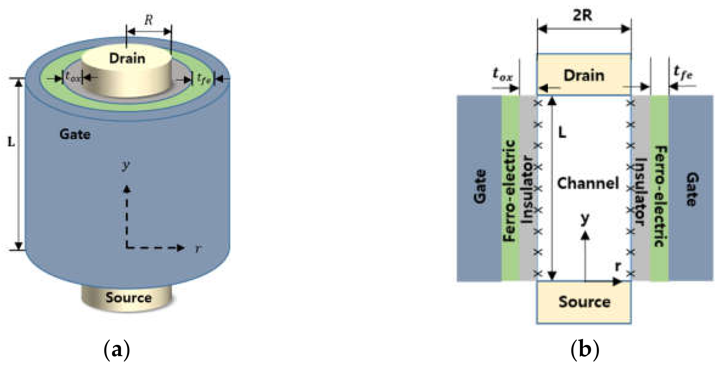
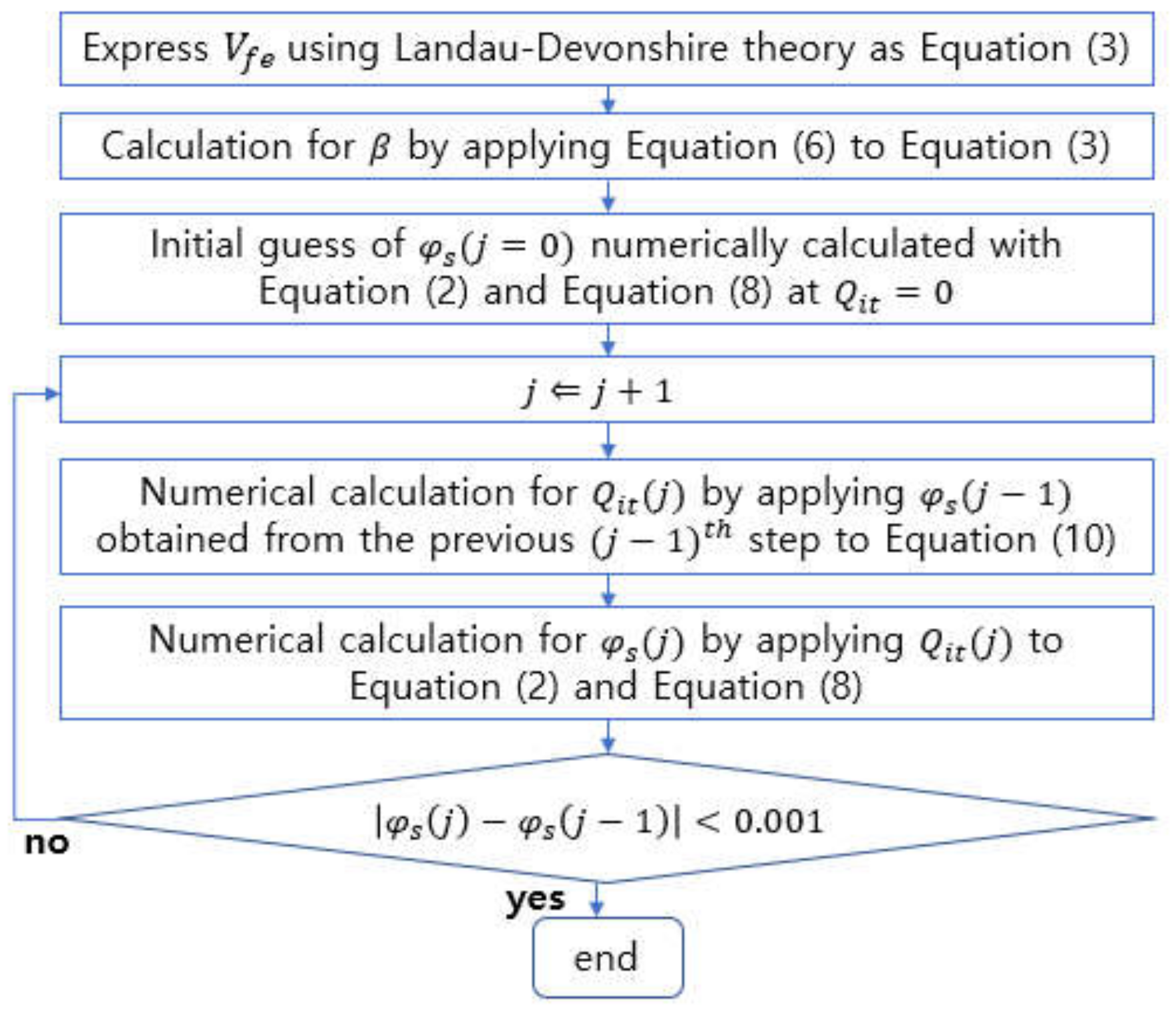
2. Method of Calculating Surface Potential of NC-GAA FET

The considered NC GAA-FET is shown in Figure 1 as an undoped channel and cylindrical GAA structure. Source and drain regions are highly doped, ignoring parasitic resistance effects in these regions. The gate stack consists of a metal gate-electrode/ferroelectric/bottom insulator/semiconductor where the bottom insulator layer is SiO2. Following the gradual channel approximation (GCA) and considering cylindrical coordinates, the general one-dimensional Poisson’s Equation of the intrinsic channel region of NC GAA-FET can be expressed as
d 2 φ d r 2 + 1 r d φ d r = q ε s i n r
where q is the electron charge, ε s i is the permittivity of the silicon channel, and n r is the free carrier charge density, which is expressed as n r = n i e x p q φ V n / k T . In this density equation, n i is the intrinsic carrier concentration, V n is the electron quasi-Fermi potential, k is the Boltzmann constant, and φ r is the electrostatic potential. Equation (1) satisfies the following boundary conditions: d φ / d r r = 0 = 0 and φ r = R = φ s , where φ s is the surface potential. According to the GCA, Vn is constant along the r-direction, i.e., Vn = Vn(y). Equation (1) can be solved analytically as in Equation (2), which is the same as the result of the GAA FET presented in previous works [15,26,27,28,29] without a ferroelectric layer.
φ r = V n 2 k T q l n R 2 β q 2 n i 2 k T ε S i 1 β 2 r 2 R 2
where R is the radius of the silicon channel, and β is the dimensionless intermediate parameter related to φ s through the secondary boundary condition. The voltage balance condition of NC-GAA FET is written as V g s = V f b Q i t C o x + φ s + V f e + V o x , where V g s is voltage across the gate-to-source, V f b is the flat-band voltage, Q i t is the interface trap charge, V f e is voltage across the ferroelectric layer, and V o x is voltage across the dielectric layer between the ferroelectric layer and silicon channel. According to Landau–Devonshire theory, V f e can be expressed in terms of mobile charge density, Q, as
V f e = a 0 Q + b 0 Q 3
where the coefficients a0 and b0 are related to the Landau parameters (a and b) of the ferroelectric material for a cylindrical gate, and they are expressed as [25]
a 0 = 2 a R ln 1 + t f e / R + t o x
b 0 = 2 b R 3 · 1 / R + t o x 2 1 / R + t f e + t o x 2
where tox is the thickness of intermediate insulator layer and tfe is the ferroelectric thickness. In addition, V o x can be expressed as V o x = Q / C o x where C o x = ε o x / R l n 1 + t o x / R .
Firstly, according to Gauss’ law, the mobile charge density, Q, can be determined, using Equation (2) as an intermediate parameter. Then the voltage balance equation can be formulated as Equation (7). This modeling methodology of the surface potential was used in [25], and this work also utilizes it and tries to write it down repeatedly to avoid confusion.
Q = ε s i d φ r d r r = R = ε S i 2 k T q 2 β 2 / R 1 β 2
V g s V f b + Q i t C o x φ s = a 0 + 1 C o x Q + b 0 Q 3
Therefore, the formula for β related to the surface potential can be obtained as in Equation (8) by substituting Q of Equation (6) into Equation (7).
l n β ln 1 β 2 + m β 2 1 β 2 + n β 2 1 β 2 3 = G
where G = q 2 k T V g s V f b + Q i t C o x V n ln 2 R 2 k T ε S i q 2 n i , m = a 0 + 1 C o x 2 ε S i R , and n = b 0 2 ε S i R 3 2 k T q 2 . Since Equation (7) is not a closed form equation, it can be solved analytically through numerical calculation to obtain an accurate solution for β, or by using advanced mathematical techniques such as the Lambert-W function [30] and asymptotic equations [25]. In this work, β was obtained by introducing an asymptotic equation and a smoothing function. In this paper, we consider only acceptor-like trap states. Interface trap charge, Q i t , can be written as Q i t = q N e t f E t , where f E t is occupation probability of an acceptor-like trap with energy level, E t is energy of single interface charge trap, and N e t is interface trap density per unit surface. By defining E t i = E t E i and using φ s = E i E F / q , interface trap charge can be obtained as Equation (10), where E i is the intrinsic fermi level energy and E F is fermi level energy.
f E t = 1 + e x p E t E F k T 1
Q i t = q N e t 1 + e x p E t i k B T e x p q φ s V n k T 1
Finally, we can solve surface potential φ s by using a self-consistent method, as shown in Figure 2, which is a similar method to previous papers of [24] that calculate the surface potential considering the interface trap in a device structure without a ferroelectric layer.

3. Analytical Drain Current Model for NC-GAA FET

We can obtain the current equation by using the drift-diffusion current equation: I d s = μ e f f 2 π R Q d V / d y . For convenience, we define α = 1 β 2 . Integrating this equation from the source to the drain and changing from the function of V to the function of α , we can obtain a different expression of the drift-diffusion current equation:
I d s = μ e f f 2 π R L 0 V d s Q V d V = μ e f f 2 π R L α s α d Q β d V d α d α
where L is the channel length, μeff is the effective mobility, and α s and α d are solved from Equation (8) corresponding to V = 0   and   V = V D S , respectively. Note that d V / d α can be expressed as a function of α by differentiating Equation (8). Substituting these factors in Equation (11), integration can be performed analytically to yield
I d s = 8 π μ e f f ε S i L k T q q N e t C o x f α D f α S + k T q g α D g α S
where new functions, f ( α ), g ( α ), are defined in Equation (10) as
f α = d a + a 1 d a 2 a + 1 2 d t a n 1 2 d a 1 4 d 1 4 d 1
w h e r e   d = e x p E t i k B T R 2 q 2 n i 2 k T ε S i 2
  g α = 2 a ln a + m 1 a 2 + 2 a + n 6   a 9 a 2 + 6 a 3 3   2 a 4
Following the approach of D. Jimenez [28], we can derive the analytical drain current Equation with closed-form by carefully checking the fluctuation of h a and a , which has different values at each operation region; h a   i s   L H S of Equation (8).
(1) Linear region above threshold
In this region, h a S ,   h a D 1 , thus a S , D   ~   1 . Hence, the term m /   a S , D 2 3 n / 2   a S , D 4 in g   a S , D becomes dominant, respectively. As a result, the drain current Equation is derived as
I d s = 8 π μ e f f ε S i L k T q q N e t C o x f α D f α S + k T q m   a D 2 3 n 2   a D 4 + m   a S 2 + 3 n 2   a S 4
(2) Saturation region above threshold
In this region, h a S 1 ,   h a D 1 , thus, a S ~   1 ,   a D   ~   0 . Hence, the term m /   a S 2 3 n / 2   a S 4 in g   a S and the term ln   a D 2 /   a D in g   a D become dominant. As a result, the drain current Equation is derived as
I d s = 8 π μ e f f ε S i L k T q q N e t C o x f α D f α S + k T q ln   a D 2 a D + m   a S 2 + 3 n 2   a S 4
(3) Subthreshold region
In this region, h a S ,   h a D 1 , thus a S ,     a D   ~   0 . Hence, the term ln   a S , D 2 /   a S , D in g   a S , D becomes dominant. As a result, the drain current Equation is derived as
I d s = 8 π μ e f f ε S i L k T q q · N e t C o x f α D f α S + k T q ln   a D 2 a D + ln   a S + 2 a S
Finally, to obtain the unified current equations, we use the smoothing function as
I d s I d s 1 , I d s 2 , ε = 2 A I d s 1 + I d s 2 + I d s 1 + I d s 2 2 A · I d s 1 · I d s 2
where A = 4 − ε and ε ∈ (0,1). In this work, a long-channel ideal characteristic model was developed using a channel length of 1 μm. By adding various short-channel effects (e.g., drain-induced barrier lowering, threshold voltage roll-off, velocity saturation, and so on) to the developed baseline model, it can be applied to devices with the channel length of several to tens of nanometers.

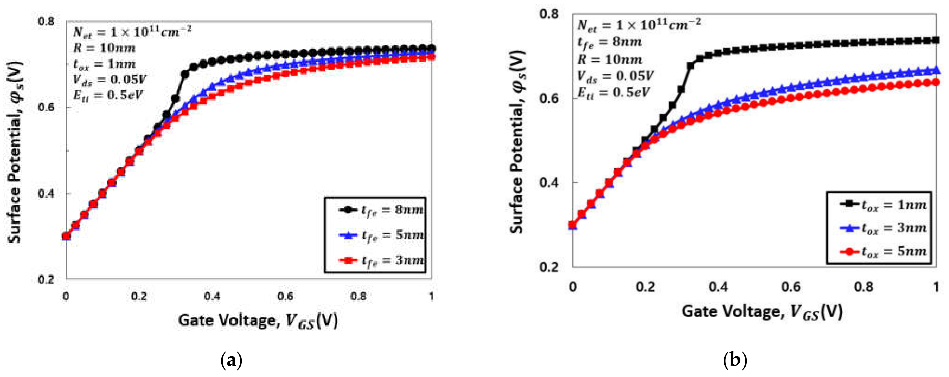
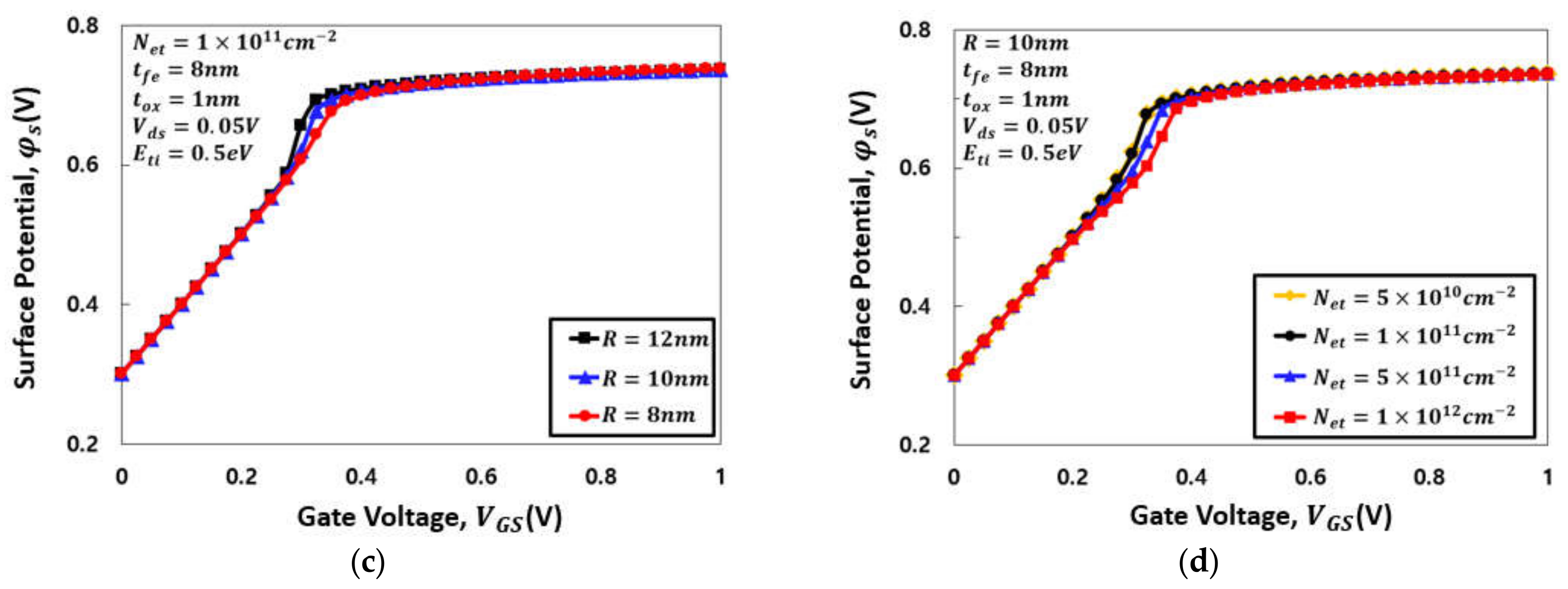
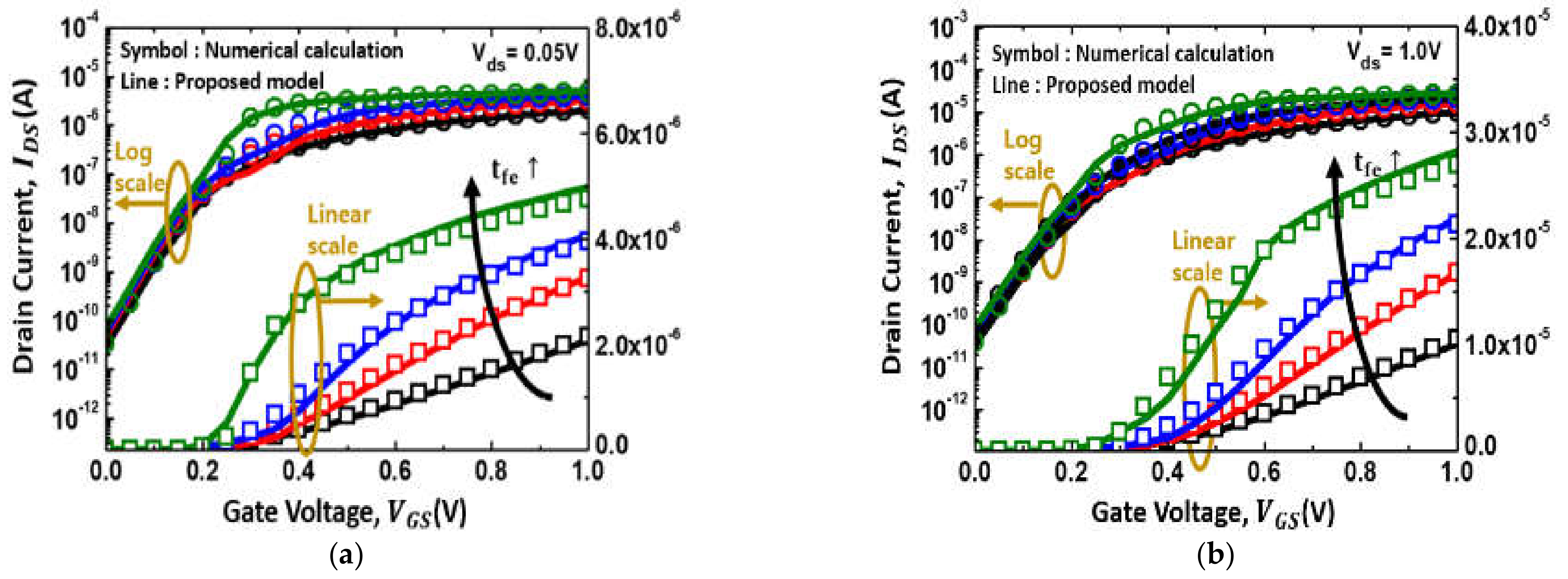
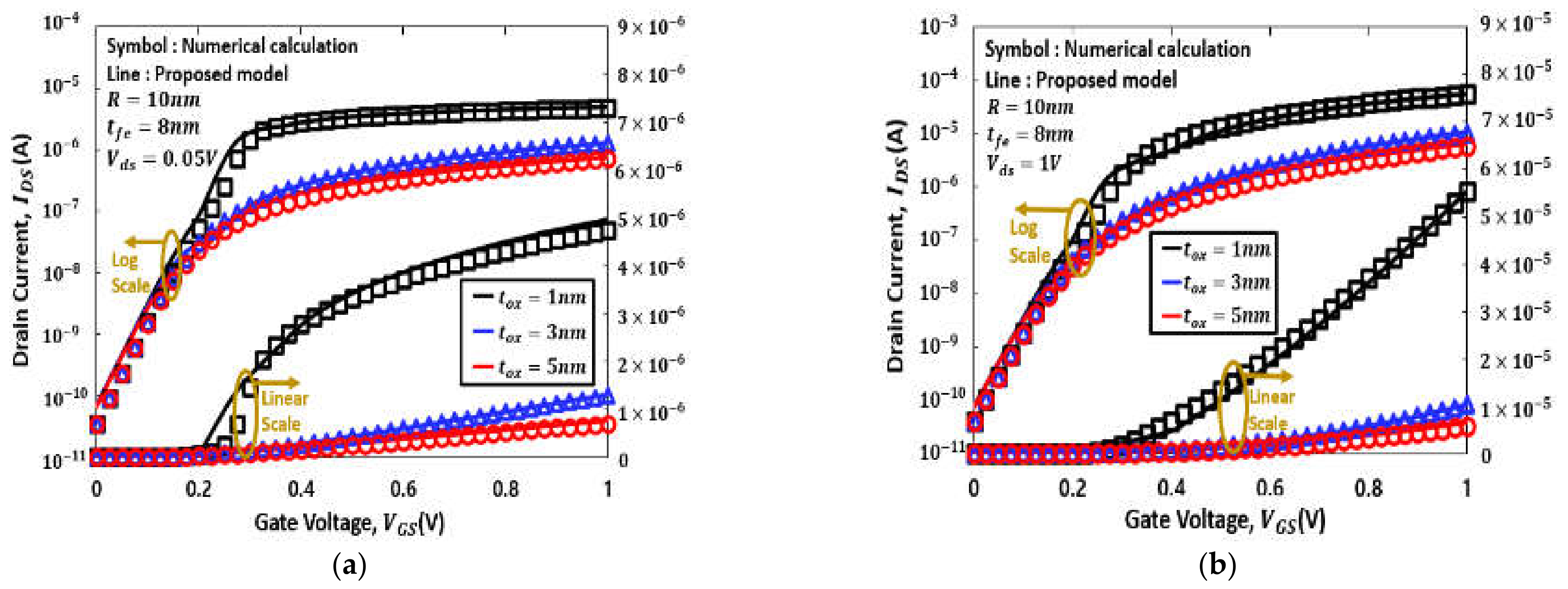
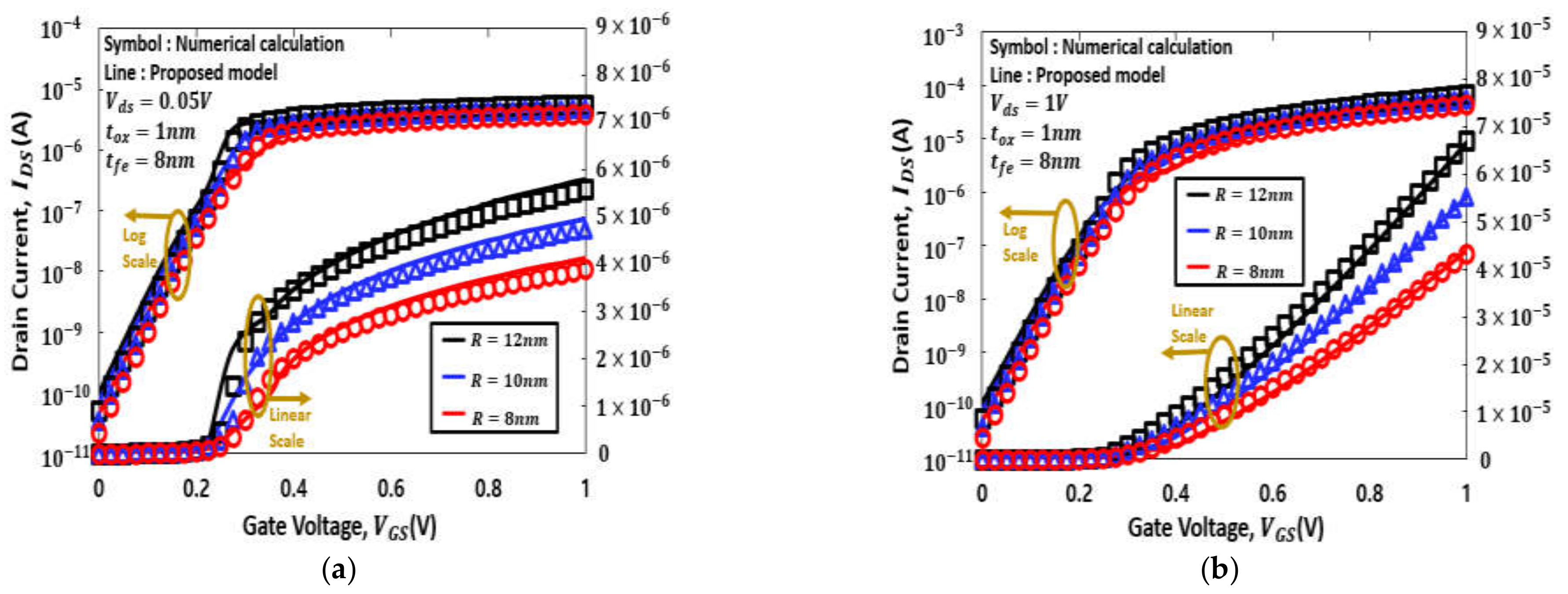
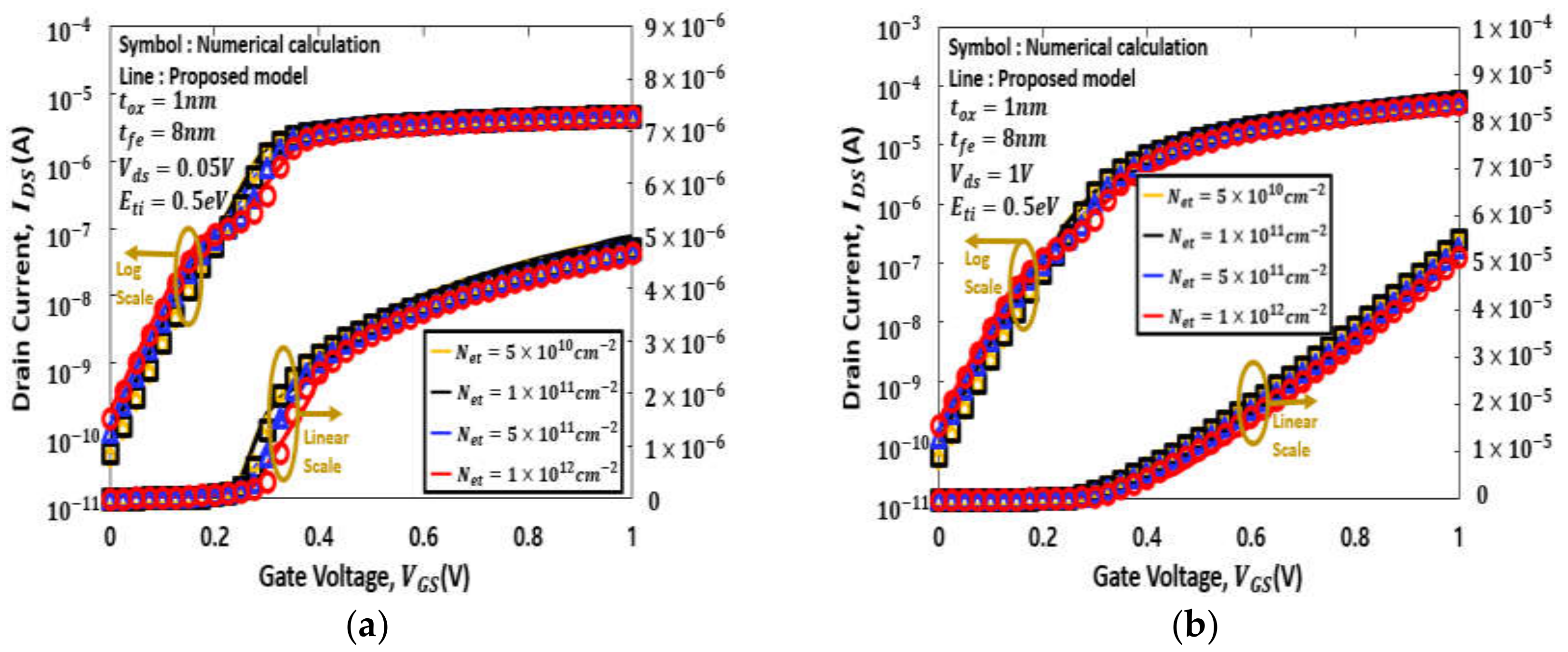
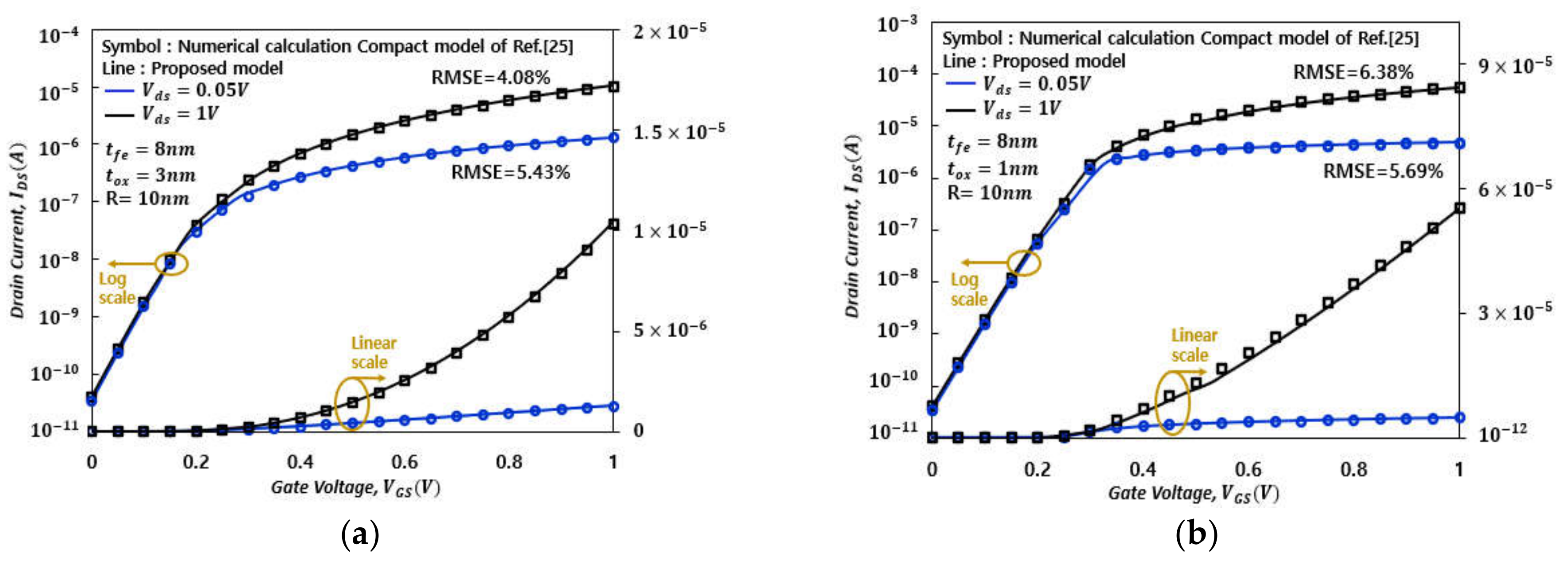
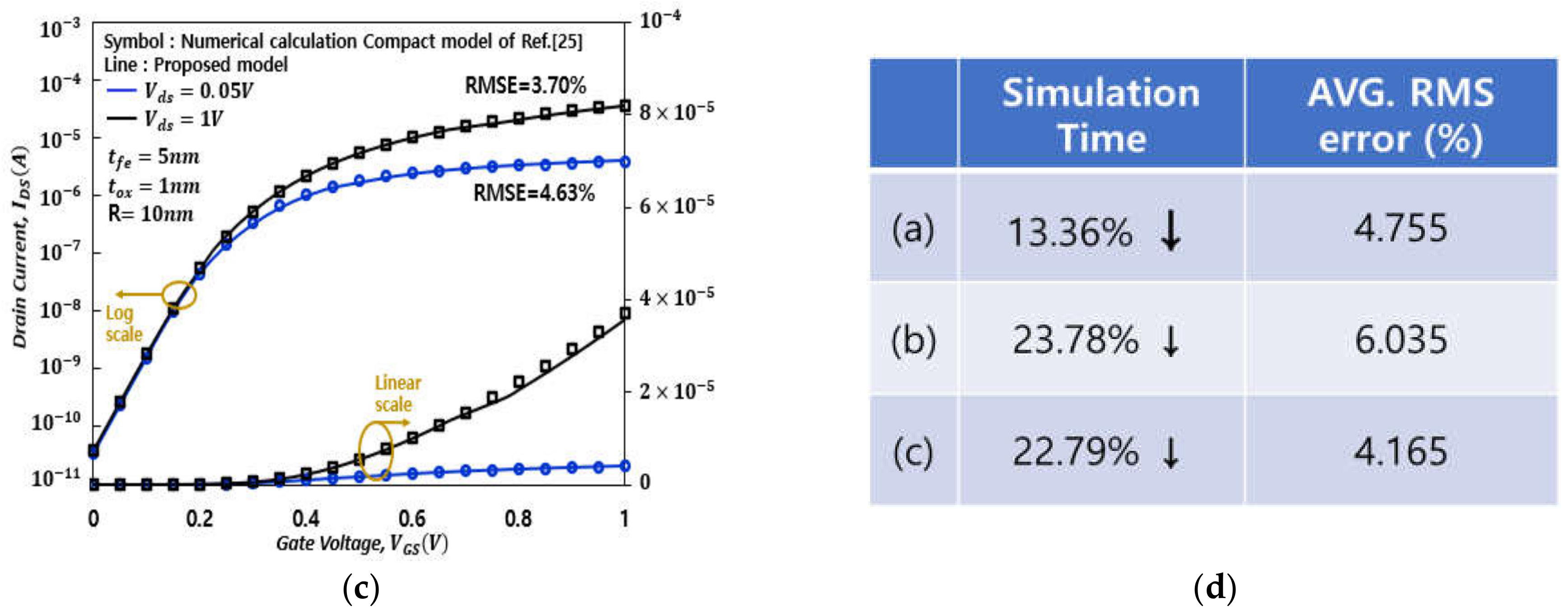
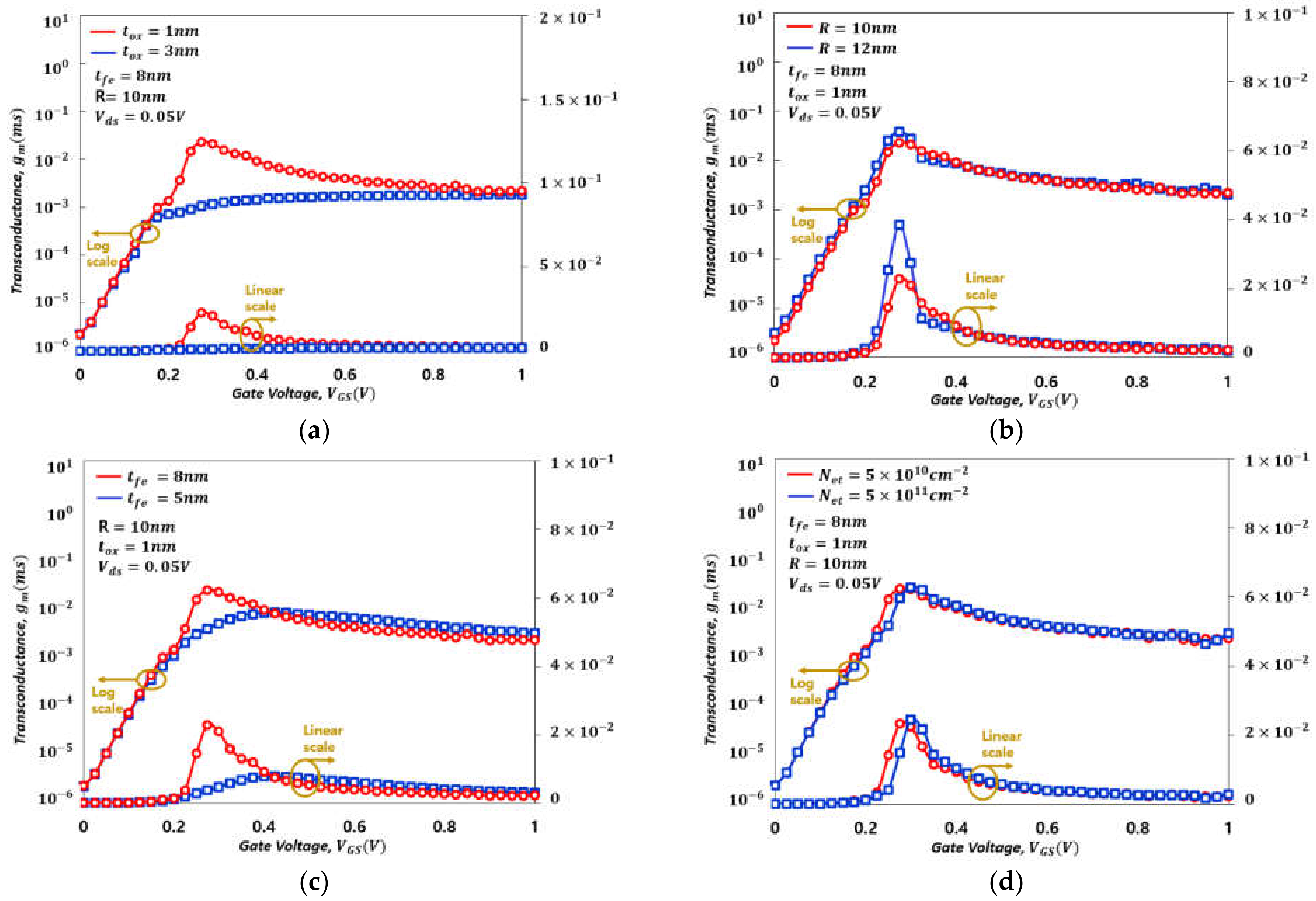
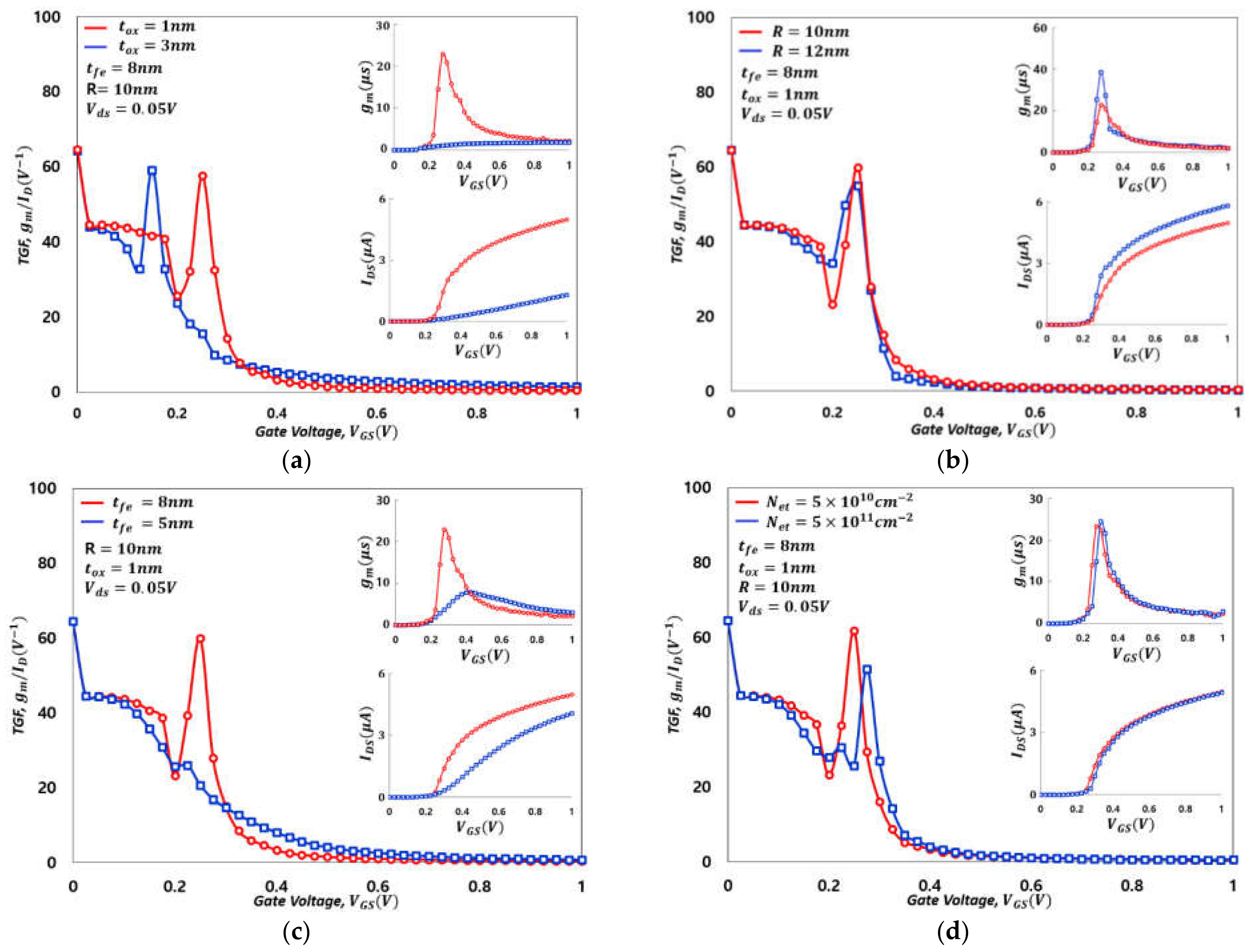
4. Results and Discussion

Table 1 shows the key dimensions and material parameters of NC GAA-FET used in the experiments. By using these parameter values, we can validate the regional-based current–voltage model and investigate electrical behaviors of NC GAA-FET in this section. In Table 1, Nsd is the doping density in source and drain regions in Table 1. As the source and drain regions are assumed to be heavily doped with N+ over 1020 cm−3, effects such as voltage drop due to parasitic resistance are neglected. Thus, 0 and Vds are applied to Vn (y) at the source end and drain end in Equations (1) and (2), respectively. This method is the same approach used for compact modeling intrinsic channel regions in previous papers [15,19,24,25,26,27,28,29,31].
The derived model is a surface potential ( φ s )-based model, and it can be calculated from Equation (8) followed by asymptotic equations. Figure 3a–d show φ s as a function of t f e , t o x , R, and N e t . As shown in Figure 3a, the surface potential increases as tfe increases, which is due to the improved capacitance matching between the ferroelectric layer and the intermediate insulator. Similarly, when the capacitance between the ferroelectric layer and the intermediate insulator deviates due to tox variation from the well-matched state, it can be seen that the voltage amplification characteristic decreases, as shown in Figure 3b. In addition, as shown in Figure 3c, although R also affects the surface potential, when 40% change based on R = 10 nm, only a slight change in the surface potential is observed. Therefore, the effects of tox and tfe are more important than R when designing the NC GAA-FET. Lastly, Figure 3d shows the effect of N e t . The surface potential increases as N e t increases, but if N e t is smaller than a certain value, we can observe that small changes occur. These surface potential characteristics directly affect the channel current characteristics shown in Figure 4, Figure 5, Figure 6 and Figure 7. In Figure 4, Figure 5, Figure 6 and Figure 7, symbols are the results of applying the complicated current–voltage model from the surface potential by the numerical analysis method proposed in the previous work [25], and the line shows the regional-based current–voltage model proposed in this work. As can be seen in Figure 4, Figure 5, Figure 6 and Figure 7, it can be seen that the proposed model in the entire operating regions of the NC GAA-FET describes the complicated current–voltage model well. Figure 4a,b show the current–voltage characteristics in low drain bias (linear region) and high drain bias (saturation region) under various tfe conditions, respectively.
As with the surface potential characteristic, it can be seen that the sub-threshold swing is improved due to the voltage amplification characteristic when it is increased up to tfe = 8 nm. Therefore, lower off current and improved operating speed can be expected at the same power supply voltage (VDD). This can be clearly confirmed by comparing current–voltage behaviors of tfe = 0 nm (GAA FET characteristics without ferroelectric layer) and tfe = 8 nm. Figure 5 shows the current–voltage characteristic when tfe is fixed and tox is increased from 1 nm (a reference state well matched with a ferroelectric layer). As tox becomes thicker, as shown in Figure 3b, the voltage amplification effect due to the NC characteristic and the current characteristic decrease due to the increase in effective oxide thickness are observed. Figure 6 shows the current–voltage characteristics when tfe and tox are fixed with the voltage amplification optimized and R increased. As R increases (decreases), there is no significant change in surface potential, as shown in Figure 3c, but the current increases (decreases) due to the effect of increasing (decreasing) the total channel width (2πR). Figure 7 shows the current–voltage characteristics when tfe, tox, and R are fixed and N e t is increased. As N e t increases (decreases) the current increases (decreases) at low gate-to-source voltage and decreases (increases) at high gate-to-source voltage.
Figure 8 is the result of comparing the model proposed in this paper with the model proposed in the previous paper of [25]. The previous result is a I–V model formula applicable to all operating regions based on surface potential calculation, and the proposed model has a complex form without considering the interface trap. On the other hand, in this work, the surface potential is calculated by considering the interface trap, and a simplified current equation is proposed according to the operating region, and an integrated model is developed by using a smoothing function. Therefore, I–V characteristics due to variations in tfe, tox, and R without interface traps can be compared with the previous results of [25]. However, the I–V characteristics according to the variation of the interface trap cannot be compared with the previous results of [25]. As shown in Figure 8, it was confirmed that the comparison result had an error of about 4–6% from that of the previous results of [25] according to the variation of various device geometries, and the computational efficiency was improved by about 13–24%. Figure 9 and Figure 10 are the results of analyzing transconductance (gm) and transconductance generation factor (TGF) using the developed model by changing various geometry (tox, tfe, and R) and trap density (Net) characteristics of NC GAA-FET. It was confirmed that the developed model can predict the first-order differential characteristics through the gm simulation results shown in Figure 9. TGF emphasizes how effectively the drain current is used to achieve better transconductance, and the variation of TGF with VGS is shown in Figure 10. When VGS increases, the TGF characteristics decrease near the threshold voltage, then increase rapidly, and then decrease monotonically in the strong inversion region.

5. Conclusions

In this work, we proposed a method to obtain the surface potential and an analytical current–voltage model of NC GAA-FET. The proposed model considers GAA cylindrical coordinates, negative capacitive effect, and interface trap at the same time. It is a channel potential-based model that calculates the surface potential between the silicon channel and the intermediate insulator. Using the obtained channel potentials and the operation regional approach, a useful and simple drain current–voltage model equation is derived by taking the appropriate approximation in each transistor’s operating region (linear, saturation, and sub-threshold regions). The proposed model shows high consistency when compared with the previous comprehensive model. In addition, the electrical properties of NC GAA-FET were investigated by varying key device parameters such as ferroelectric thickness, intermediate insulator thickness, silicon channel radius, and interface trap density per unit surface.

Author Contributions

Y.K. contributed to the main idea and writing of this research. Y.S., S.K., J.K., S.B. performed the simulations. I.Y., C.Y., J.H. (Junghoon Ham), J.H. (Jungmin Hong) contributed to the verifications and researching of the previous works. This research activity was planned and executed under the supervision of J.J. All authors have read and agreed to the published version of the manuscript.

Funding

This work was supported by a National Foundation of Korea (NRF) grant funded by the Korea government (MIST) (No. 2020M3F3A2A01081595), and partly by a National Foundation of Korea (NRF) grant funded by the Korea government (MIST) (No. 2020M3F3A2A01082326).

Acknowledgments

The EDA tool was supported by the IC Design Education Center (IDEC), Korea. This paper was supported by the Konkuk University Researcher Fund in 2019.

Conflicts of Interest

The authors declare no conflict of interest.

References

  1. Lee, S.-Y.; Kim, S.-M.; Yoon, E.-J.; Oh, C.-W.; Chung, I.; Park, D.; Kim, K. A novel multibridge-channel MOSFET (MBCFET): Fabrication technologies and characteristics. IEEE Trans. Nanotechnol. 2003, 2, 253–257. [Google Scholar] [CrossRef]
  2. Barraud, S.; Lapras, V.; Previtali, B.; Samson, M.P.; Lacord, J.; Martinie, S.; Jaud, M.-A.; Athanasiou, S.; Triozon, F.; Rozeau, O.; et al. Performance and design considerations for gate-all-around stacked-nanowires FETs. In Proceedings of the 2017 IEEE International Electron Devices Meeting (IEDM), San Francisco, CA, USA, 2–6 December 2017; IEEE: Piscataway, NJ, USA, 2017. [Google Scholar]
  3. Bae, M.S.; Yun, I. Compact modeling of the subthreshold characteristics of junctionless double-gate FETs including the source/drain extentsion regions. Solid-State Electron. 2019, 156, 48. [Google Scholar] [CrossRef]
  4. Pezzimenti, F. Modeling of the Steady State and Switching Characteristics of a Normally Off 4H-SiC Trench Bi-polar-Mode FET. IEEE Trans. Electron Dev. 2013, 60, 1404. [Google Scholar] [CrossRef]
  5. Pezzimenti, F.; Bencherif, H.; Yousfi, A.; Dehimi, L. Current-voltage analytical model and multiobjective optimization of design of a short channel gate-all-around-junctionless MOSFET. Solid-State Electron. 2019, 161, 107642. [Google Scholar] [CrossRef]
  6. Xu, H.F.; Guan, B.G. Two-dimensional analytical model for hetero-juncion double-gate tunnel field-effect transistor with a stacked gate-oxide structure. Jpn. J. Appl. Phys. 2017, 56, 054201. [Google Scholar] [CrossRef]
  7. Jang, D.; Yakimets, D.; Eneman, G.; Schuddinck, P.; Bardon, M.G.; Raghavan, P.; Spessot, A.; Verkest, D.; Mocuta, A. Device Exploration of NanoSheet Transistors for Sub-7-nm Technology Node. IEEE Trans. Electron Devices 2017, 64, 2707–2713. [Google Scholar] [CrossRef]
  8. Yakimets, D.; Bardon, M.G.; Jang, D.; Schuddinck, P.; Sherazi, Y.; Weckx, P.; Miyaguchi, K.; Parvais, B.; Raghavan, P.; Spessot, A.; et al. Power aware FinFET and lateral nanosheet FET targeting for 3nm CMOS technology. In Proceedings of the 2017 IEEE International Electron Devices Meeting (IEDM), San Francisco, CA, USA, 2–6 December 2017; Institute of Electrical and Electronics Engineers (IEEE): Piscataway, NJ, USA, 2017; pp. 20.4.1–20.4.4. [Google Scholar]
  9. Danowitz, A.; Kelley, K.; Mao, J.; Stevenson, J.P.; Horowitz, M. CPU DB: Recording Microprocessor History. Queue 2012, 10, 10–27. [Google Scholar] [CrossRef]
  10. Hilbert, M.; López, P. The World’s Technological Capacity to Store, Communicate, and Compute Information. Science 2011, 332, 60–65. [Google Scholar] [CrossRef] [Green Version]
  11. Lee, M.H.; Fan, S.-T.; Tang, C.-H.; Chen, P.-G.; Chou, Y.-C.; Chen, H.-H.; Kuo, J.-Y.; Xie, M.-J.; Liu, S.-N.; Liao, M.-H.; et al. Physical thickness 1.x nm ferroelectric HfZrOx negative capacitance FETs. In Proceedings of the 2016 IEEE International Electron Devices Meeting (IEDM), San Francisco, CA, USA, 3–7 December 2016; IEEE: Piscataway, NJ, USA, 2016; pp. 12.1.1–12.1.4. [Google Scholar]
  12. Khan, A.I.; Yeung, C.W.; Hu, C.; Salahuddin, S. Ferroelectric negative capacitance MOSFET: Capacitance tuning & antiferroelectric operation. In Proceedings of the 2011 International Electron Devices Meeting, Washington, DC, USA, 5–7 December 2011; Institute of Electrical and Electronics Engineers (IEEE): Piscataway, NJ, USA, 2011; pp. 11.3.1–11.3.4. [Google Scholar]
  13. Lin, C.-I.; Khan, A.I.; Salahuddin, S.; Hu, C. Effects of the Variation of Ferroelectric Properties on Negative Capacitance FET Characteristics. IEEE Trans. Electron Devices 2016, 63, 2197–2199. [Google Scholar] [CrossRef]
  14. Krishnamohan, T.; Kim, D.; Raghunathan, S.; Saraswat, K. Double-Gate Strained-Ge Heterostructure Tunneling FET (TFET) With record high drive currents and ≪ 60mV/dec subthreshold slope. In Proceedings of the 2008 IEEE International Electron Devices Meeting, San Francisco, CA, USA, 15–17 December 2008; IEEE: Piscataway, NJ, USA, 2008; pp. 1–3. [Google Scholar]
  15. Vishnoi, R.; Kumar, M.J. Compact Analytical Drain Current Model of Gate-All-Around Nanowire Tunneling FET. IEEE Trans. Electron. Devices 2014, 61, 2599–2603. [Google Scholar] [CrossRef]
  16. Knoch, J.; Mantl, S.; Appenzeller, J. Impact of the dimensionality on the performance of tunneling FETs: Bulk versus one-dimensional devices. Solid-State Electron. 2007, 51, 572–578. [Google Scholar] [CrossRef]
  17. Dunga, M.V.; Morshed, T.H.; Darsen, D.L.; Wenwei, Y.; Xuemei, X.; He, J.; Liu, W.; Cao, K.M.; Jin, X.; Ou, J.J.; et al. Bsim4. 6.0 Mosfet Model; University of California: Berkeley, CA, USA, 2006. [Google Scholar]
  18. Dunga, M.V.; Lin, C.-H.; Niknejad, A.M.; Hu, C. BSIM-CMG: A Compact Model for Multi-Gate Transistors. In FinFETs and Other Multi-Gate Transistors; Springer: Berlin/Heidelberg, Germany, 2007; pp. 113–153. [Google Scholar]
  19. Pahwa, G.; Dutta, T.; Agarwal, A.; Chauhan, Y.S. Compact Model for Ferroelectric Negative Capacitance Transistor with MFIS Structure. IEEE Trans. Electron Devices 2017, 64, 1366–1374. [Google Scholar] [CrossRef]
  20. Kobayashi, M.; Ueyama, N.; Jang, K.; Hiramoto, T. Experimental study on polarization-limited operation speed of negative capacitance FET with ferroelectric HfO2. In Proceedings of the 2016 IEEE International Electron Devices Meeting, San Francisco, CA, USA, 3–7 December 2016; IEEE: Piscataway, NJ, USA, 2016; pp. 12.3.1–12.3.4. [Google Scholar]
  21. Kim, T.; Shin, C. Effects of Interface Trap on Transient Negative Capacitance Effect: Phase Field Model. Electronics 2020, 9, 2141. [Google Scholar] [CrossRef]
  22. Lee, H.-P.; Tseng, K.-Y.; Su, P. Interface discrete trap induced variability for negative capacitance FinFETs. In Proceedings of the 2018 International Symposium on VLSI Technology, Systems and Application (VLSI-TSA), Hsinchu, Taiwan, 16–19 April 2018; Institute of Electrical and Electronics Engineers (IEEE): Piscataway, NJ, USA, 2018; pp. 1–2. [Google Scholar]
  23. Prakash, O.; Gupta, A.; Pahwa, G.; Henkel, J.; Chauhan, J.H.Y.S.; Amrouch, H. Impact of Interface Traps on Negative Capacitance Transistor: Device and Circuit Reliability. IEEE J. Electron Devices Soc. 2020, 8, 1193–1201. [Google Scholar] [CrossRef]
  24. Najam, F.; Yu, Y.S.; Cho, K.H.; Yeo, K.H.; Kim, D.-W.; Hwang, J.S.; Kim, S.; Hwang, S.W. Interface Trap Density of Gate-All-Around Silicon Nanowire Field-Effect Transistors with TiN Gate: Extraction and Compact Model. IEEE Trans. Electron Devices 2013, 60, 2457–2463. [Google Scholar] [CrossRef]
  25. Gaidhane, A.D.; Pahwa, G.; Verma, A.; Chauhan, Y.S. Compact Modeling of Drain Current, Charges, and Capacitances in Long-Channel Gate-All-Around Negative Capacitance MFIS Transistor. IEEE Trans. Electron Devices 2018, 65, 2024–2032. [Google Scholar] [CrossRef]
  26. Iniguez, B.; Fjeldly, T.; Lazaro, A.; Danneville, F.; Deen, M. Compact-Modeling Solutions for Nanoscale Double-Gate and Gate-All-Around MOSFETs. IEEE Trans. Electron Devices 2006, 53, 2128–2142. [Google Scholar] [CrossRef]
  27. Jimenez, D.; Iniguez, B.; Sune, J.; Marsal, L.; Pallares, J.; Roig, J.; Flores, D. Continuous Analytic I–V Model for Surrounding-Gate MOSFETs. IEEE Electron Device Lett. 2004, 25, 571–573. [Google Scholar] [CrossRef]
  28. Duarte, J.P.; Choi, S.-J.; Moon, D.-I.; Ahn, J.-H.; Kim, J.-Y.; Kim, S.; Choi, Y.-K. A Universal Core Model for Multiple-Gate Field-Effect Transistors. Part II: Drain Current Model. IEEE Trans. Electron Devices 2013, 60, 848–855. [Google Scholar] [CrossRef]
  29. Seon, Y.; Kim, J.; Kim, S.; Jeon, J. Analytical Current-Voltage Model for Gate-All-Around Transistor with Poly-Crystalline Silicon Channel. Electronics 2019, 8, 988. [Google Scholar] [CrossRef] [Green Version]
  30. Corless, R.M.; Gonnet, G.H.; Hare, D.E.G.; Jeffrey, D.J.; Knuth, D.E. On the Lambert W function. Advances in Computational mathematics. Adv. Comput. Math. 1996, 5, 329–359. [Google Scholar] [CrossRef]
  31. Duarte, J.P.; Khandelwal, S.; Khan, A.I.; Sachid, A.; Lin, Y.-K.; Chang, H.-L.; Salahuddin, S.; Hu, C. Compact models of negative-capacitance FinFETs: Lumped and distributed charge models. In Proceedings of the 2016 IEEE International Electron Devices Meeting (IEDM), San Francisco, CA, USA, 3–7 December 2016; IEEE: Piscataway, NJ, USA, 2016; pp. 30.5.1–30.5.4. [Google Scholar]
Figure 1. (a) Three-dimensional scheme of the NC-GAA FET; (b) cross-section of the NC-GAA FET.
Electronics 10 01177 g001
Figure 2. Flowchart for surface potential and interface trap charge of NC-GAA FET using self-consistent calculation.
Electronics 10 01177 g002
Figure 3. Electrostatic surface potential versus gate-to-source voltage (a) varies with ferro-electric material thickness; (b) varies with oxide thickness; (c) varies with radius; and (d) varies with interface trap density per unit surface.
Electronics 10 01177 g003aElectronics 10 01177 g003b
Figure 4. Comparison of drain current versus gate-to-source voltage between proposed model and numerical calculation when ferro-electric thickness varies with t f e = 0, 3, 5, and 8 nm (R = 10 nm, t o x   = 1 nm); (a) low drain bias; (b) high drain bias.
Electronics 10 01177 g004
Figure 5. Result of drain current versus gate-to-source voltage when oxide thickness varies with t o x = 1, 3, and 5 nm; (a) low drain bias; (b) high drain bias.
Electronics 10 01177 g005
Figure 6. Result of drain current versus gate-to-source voltage when radius varies with R = 8, 10, and 12 nm; (a) low drain bias; (b) high drain bias.
Electronics 10 01177 g006
Figure 7. Result of drain current versus gate-to-source voltage when interface trap density per unit surface varies with Net = 5 × 10¹⁰, 1 × 10¹¹, 5 × 10¹¹, 1 × 10¹²; (a) low drain bias; (b) high drain bias.
Electronics 10 01177 g007
Figure 8. Comparison of IDS–VGS prediction results between the previous work [25] and this work for various geometry cases; (a) tfe = 8 nm, tox = 3 nm, R = 10 nm, (b) tfe = 8 nm, tox = 1 nm, R = 10 nm, (c) tfe = 5 nm, tox = 1 nm, R = 10 nm, and (d) summary of simulation time and average root-mean-square (RMS) error.
Electronics 10 01177 g008aElectronics 10 01177 g008b
Figure 9. Characteristics of transconductance (gm) for various geometries; (a) tox, (b) R, (c) tfe, and trap density (d) Net.
Electronics 10 01177 g009
Figure 10. Characteristics of transconductance generation factor (TGF) for various geometries; (a) tox, (b) R, (c) tfe, and trap density (d) Net.
Electronics 10 01177 g010
Table 1. Parameter symbols and values.
Symbol (Units)ValueFerroelectric Parameter [31]
L μ m 1a = −3 × 10⁹ m/F in Equation (4)
b = 6 × 10¹¹ m5/C2F in Equation (5)
which is corresponding coercive field Ec = 1.15 MV/cm and remnant polarization Pr = 5 μC/cm2
R n m 8–12
t f e   n m 3–8
t o x   n m 1–5
V f b   V −0.3
μ e f f   c m 2 V 1 s 1 300
N e t c m 2 0–1 × 10 12
N s d c m 3 >1020
Publisher’s Note: MDPI stays neutral with regard to jurisdictional claims in published maps and institutional affiliations.

