
An 8–12.5-GHz LC PLL with Dual VCO and Noise-Reduced LDO Regulator for Multilane Multiprotocol SerDes in 28-nm CMOS Technology


Abstract
:1. Introduction
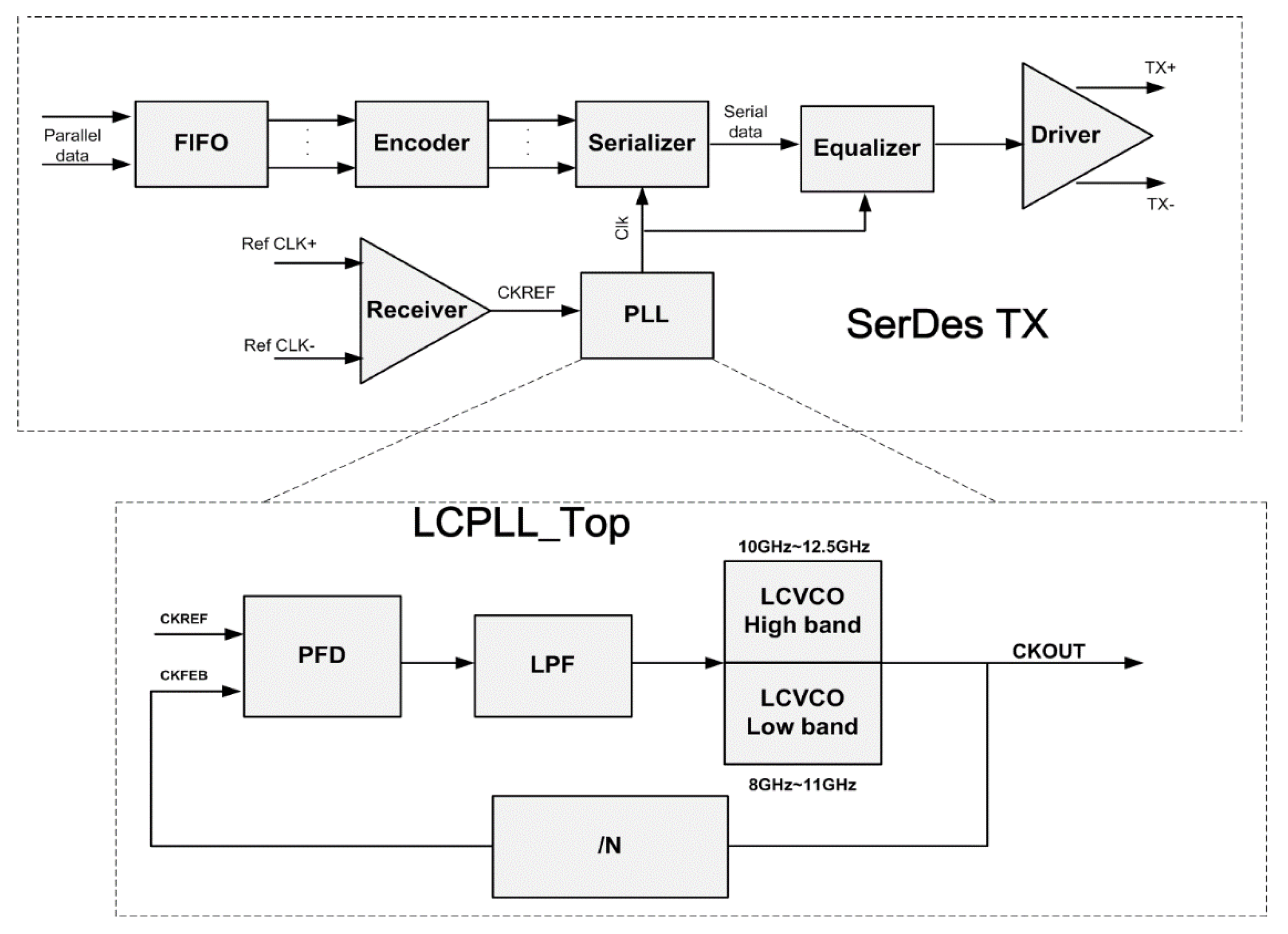
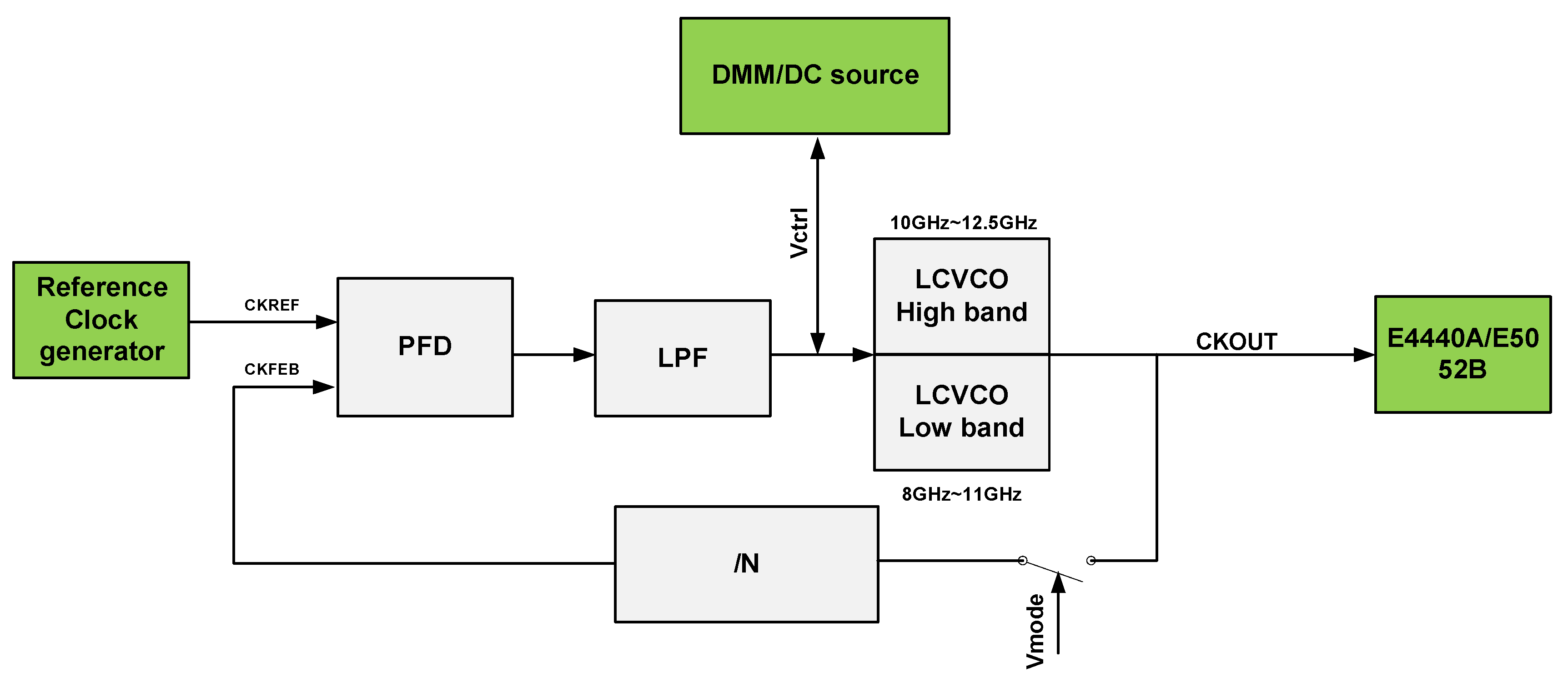
2. LC PLL Design
2.1. LC PLL Structure
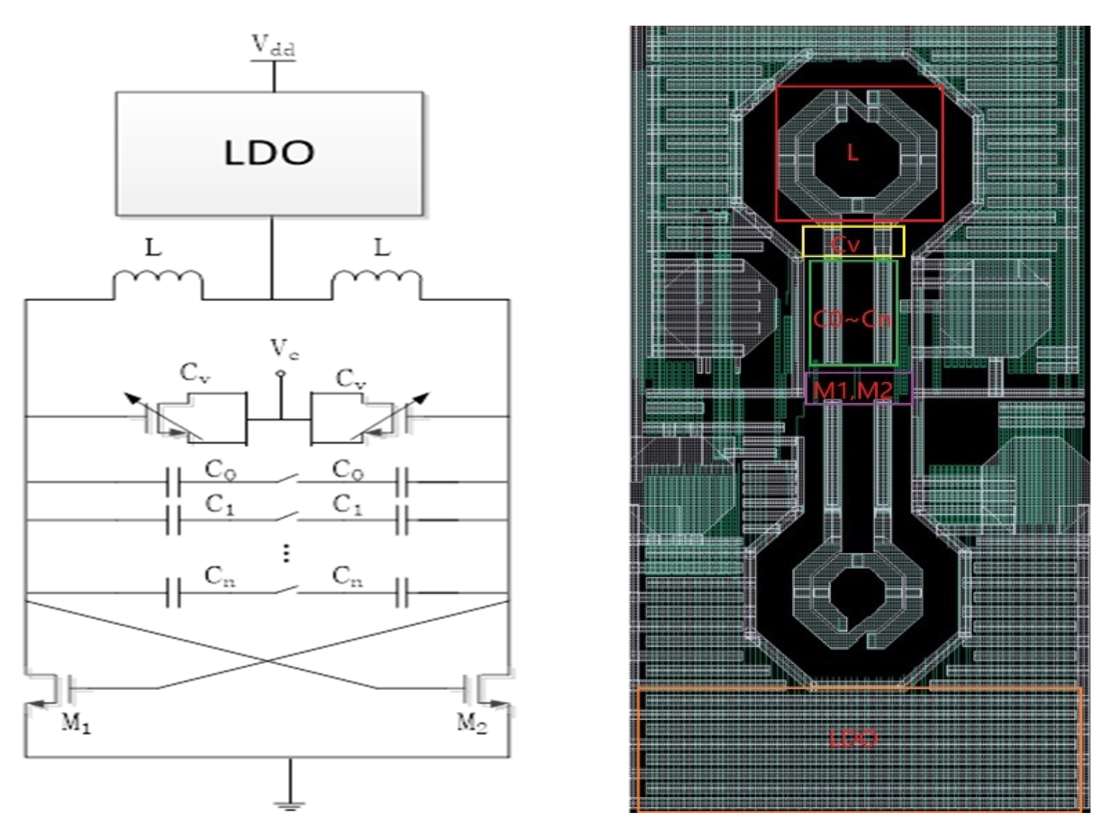
2.2. LC VCO Structure and Noise Analysis
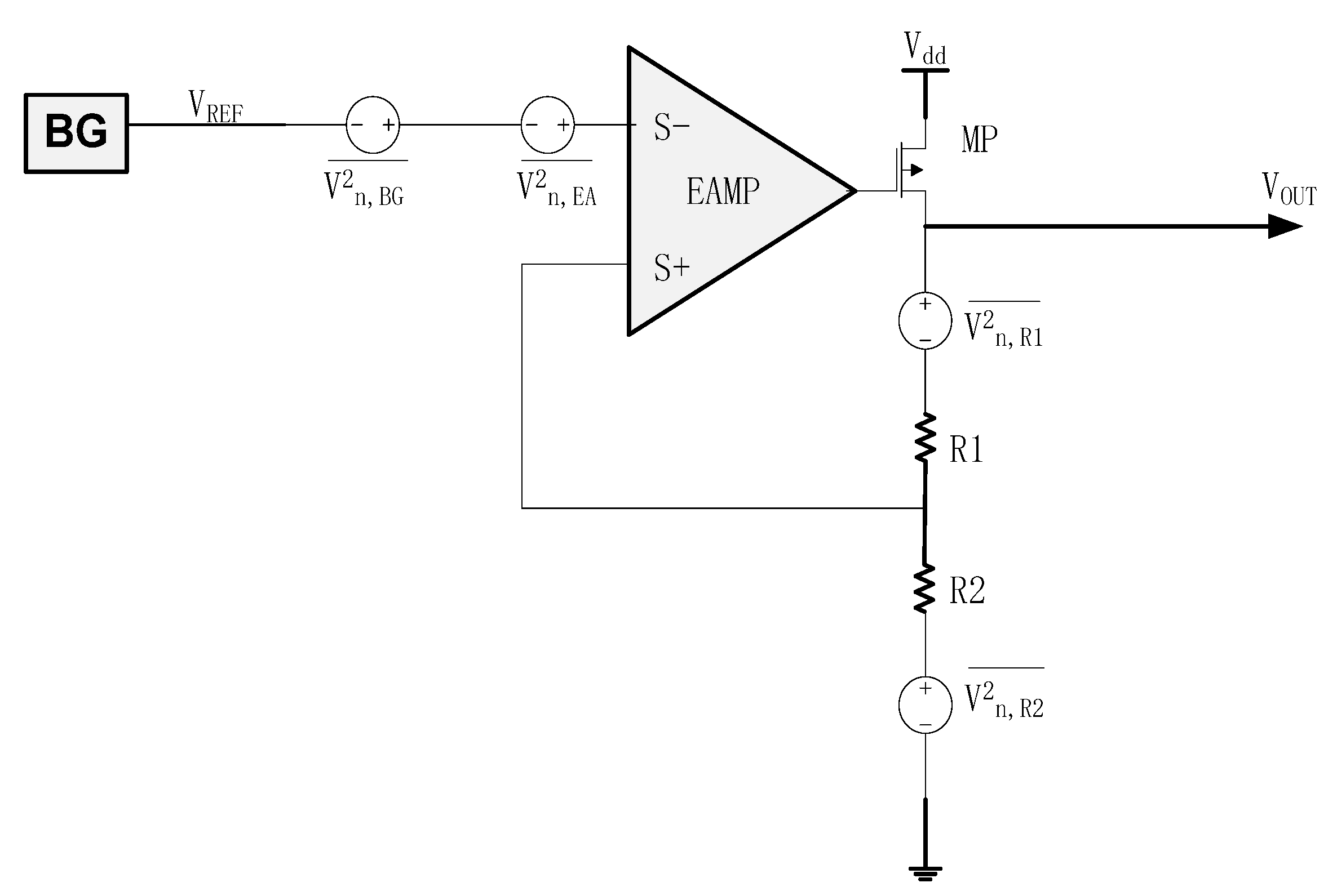
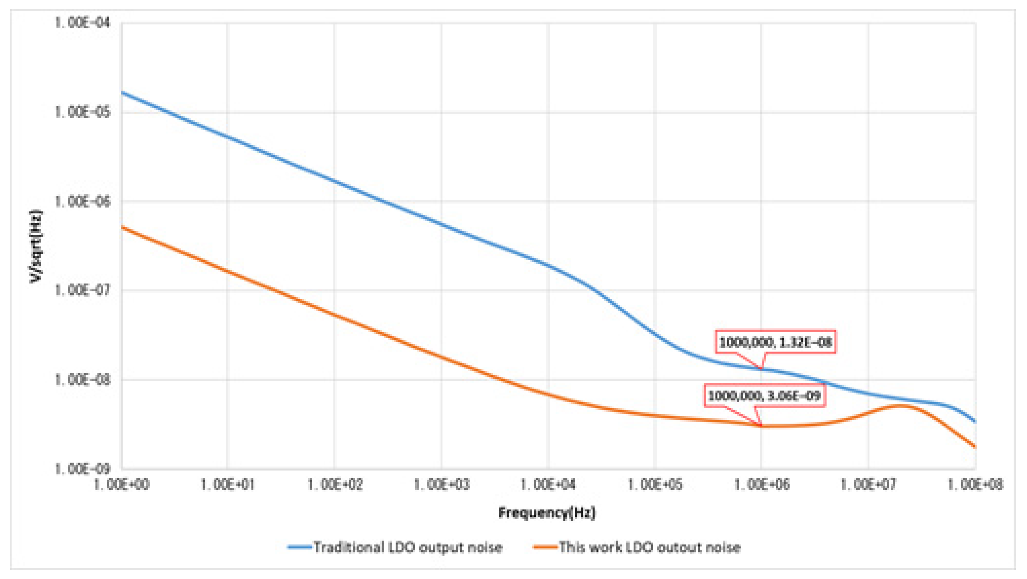
2.3. Noise-Reduced LDO Design
3. Post-Simulation and Measurement Results
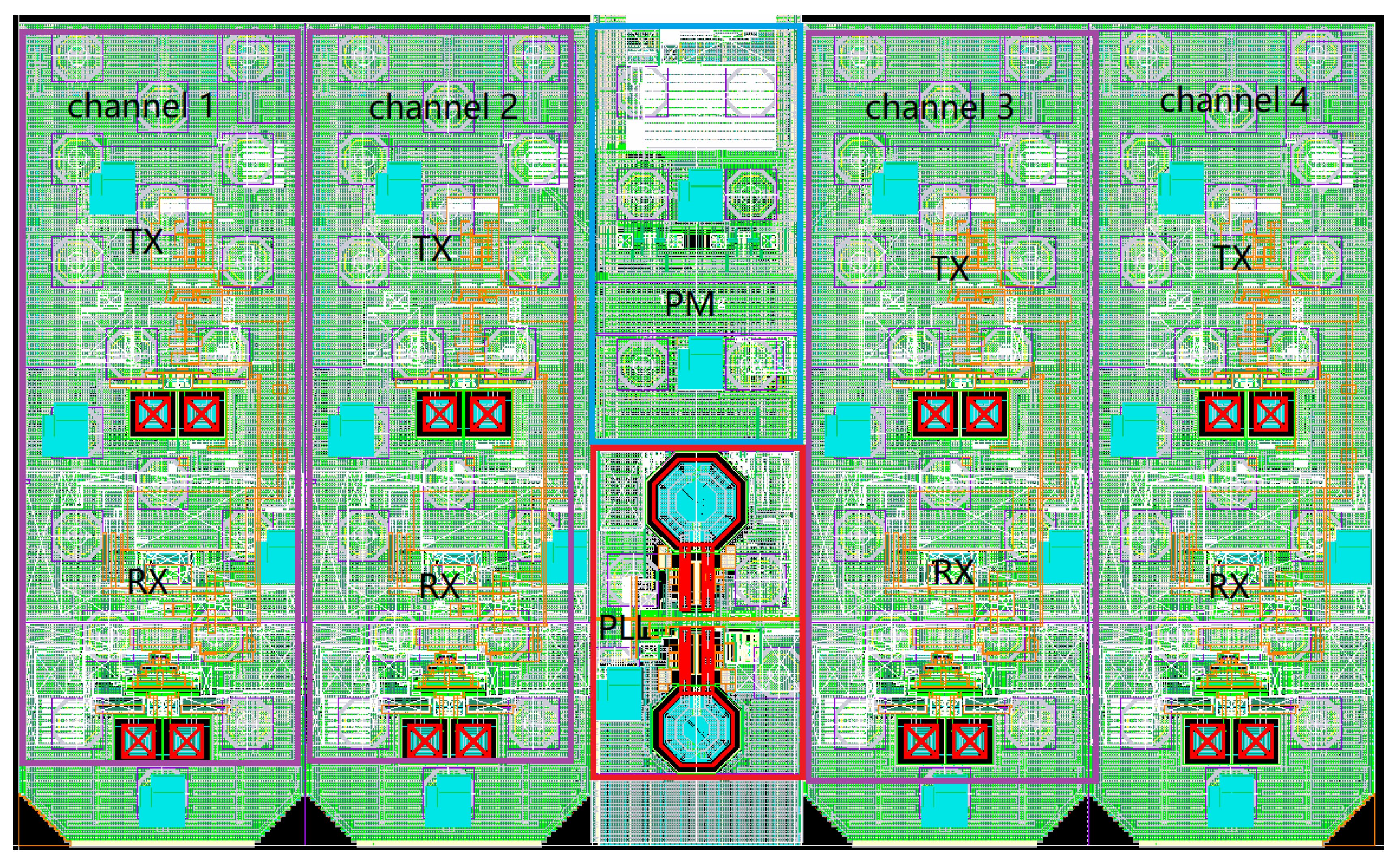
3.1. Low-Noise LC PLL Layout
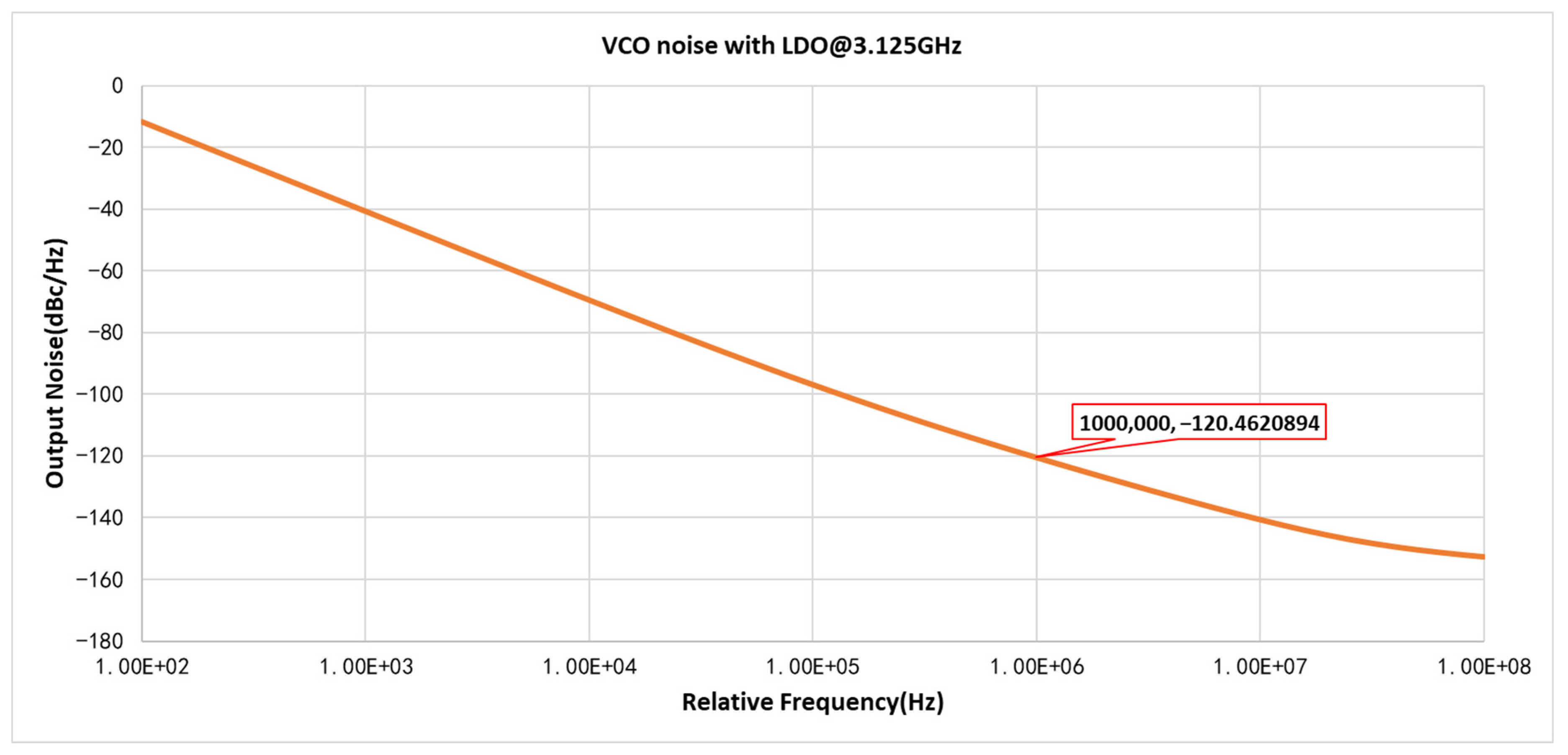
3.2. VCO Noise
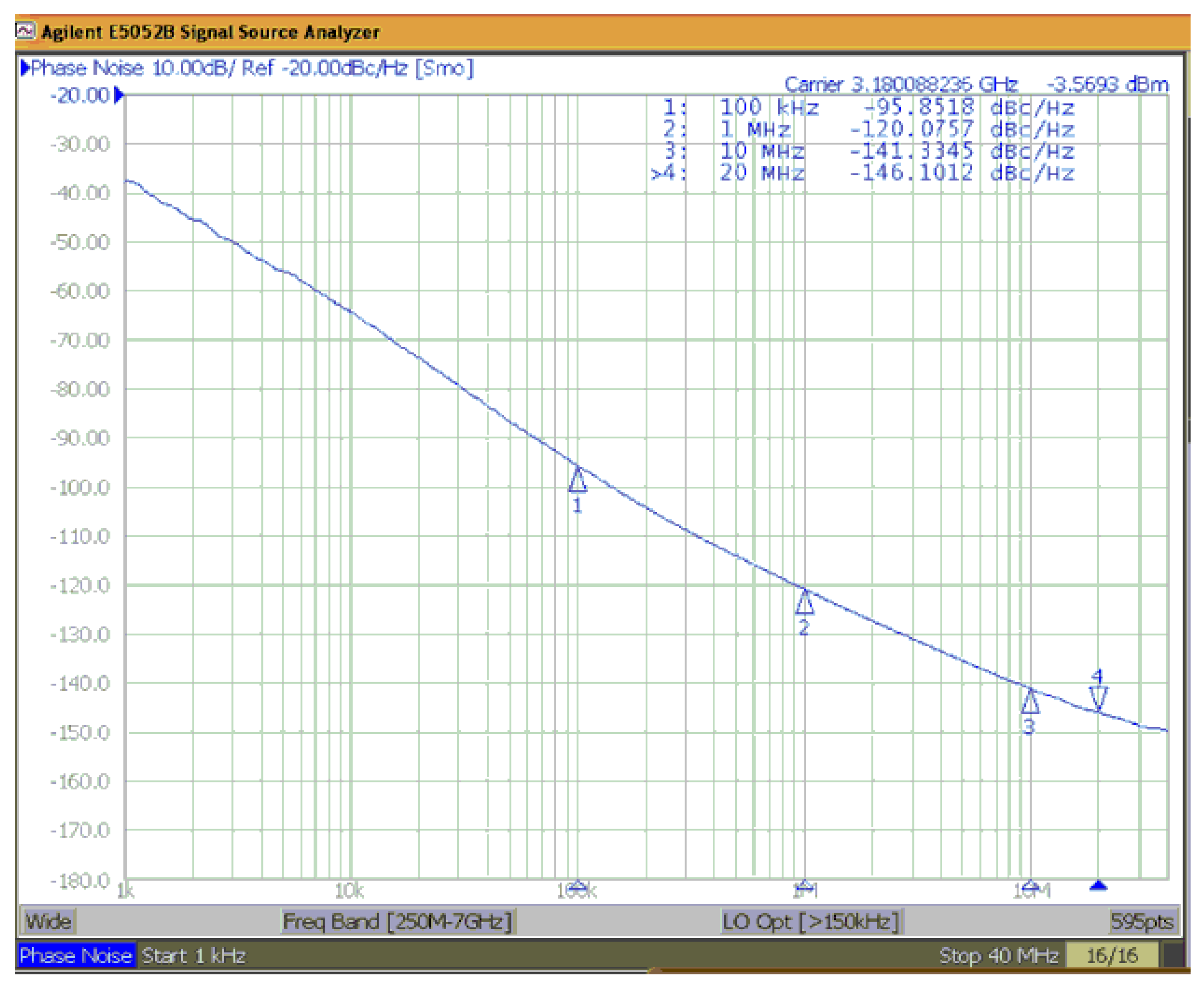
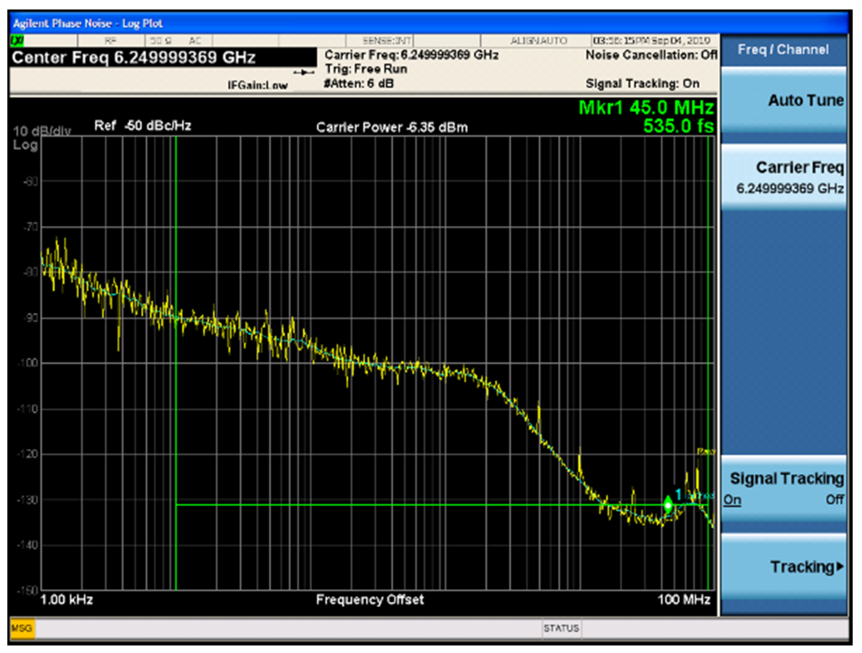
3.3. LC PLL Noise
3.4. Calculation of the LC VCO Figure of Merit (FOM) Value
3.5. Performance Summary
4. Conclusions
Author Contributions
Funding
Data Availability Statement
Conflicts of Interest
References
- Cevrero, A.; Ozkaya, I.; Francese, P.A.; Brandli, M.; Menolfi, C.; Morf, T.; Kossel, M.; Kull, L.; Luu, D.; Dazzi, M.; et al. A 100Gb/s 1.1pJ/b PAM-4 RX with Dual-Mode 1-Tap PAM-4/3-Tap NRZ Speculative DFE in14 nm CMOS FinFET. In Proceedings of the 2019 IEEE International Solid-State Circuits Conference (ISSCC), San Francisco, CA, USA, 17–21 February 2019; pp. 112–113. [Google Scholar]
- LaCroix, M.-A.; Wong, H.; Hua, Y.L.; Ho, H.; Lebedev, S.; Krotnev, P.; Nicolescu, D.A.; Petrov, D.; Carvalho, C.; Alie, S.; et al. A 60Gb/s PAM-4 ADC-DSP Transceiverin 7 nm CMOS with SNR-Based Adaptive Power ScalingAchieving 6.9 pJ/b at 32dB Loss. In Proceedings of the 2019 IEEE International Solid-State Circuits Conference (ISSCC), San Francisco, CA, USA, 17–21 February 2019; pp. 114–116. [Google Scholar]
- Hong, J.-P. A low supply voltage and wide-tuned CMOS Colpitts VCO. IEICE Electron. Express 2014, 11, 20140428. [Google Scholar] [CrossRef] [Green Version]
- Wang, T.-P.; Chiang, C.-Y. A low-power low-phase-noise wide-tuning-range K-band VCO in 0.18 μm CMOS. IEICE Electron. Express 2011, 8, 1511–1518. [Google Scholar] [CrossRef] [Green Version]
- Cameron, R.J.; Yu, M.; Wang, Y. Direct-coupled microwave filters with single and dual stopbands. IEEE Trans. Microw. Theory Tech. 2005, 53, 3288. [Google Scholar] [CrossRef]
- Noruzpur, F.; Mahdavi, S.; Poreh, M.; Ghasemi, S.T. A New Semi-Digital Low Power Low Jitter and Fast PLL in 0.18 μm Technology. In Proceedings of the 2018 25th International Conference Mixed Design of Integrated Circuits and System (MIXDES), Gdynia, Poland, 21–23 June 2018. [Google Scholar]
- Gao, X. Low jitter and low power PLL: Towards the Utopia. In Proceedings of the 2019 International SoC Design Conference (ISOCC), Jeju, Korea, 6–9 October 2019; pp. 2163–9612. [Google Scholar]
- Ebrahimi, E.; Naseh, S. A new low-phase noise direct-coupled CMOS LC-QVCO. IEICE Electron. Express 2009, 6, 1337–1344. [Google Scholar] [CrossRef] [Green Version]
- Yang, Z.-Y.; Chen, R.Y. High-performance cost-efficient dual-band CMOS LC VCO. IEICE Electron. Express 2015, 12, 20150118. [Google Scholar] [CrossRef] [Green Version]
- Kim, J.; Park, J.; Kim, J. A Low Phase Noise 0.9–1.8 GHz Dual-band LC VCO in 0.18 μm CMOS Technology. In Proceedings of the 2018 International Conference on Electronics, Information, and Communication (ICEIC), Honolulu, HI, USA, 24–27 January 2018; ISBN 978-1-5386-4754-7. [Google Scholar]
- Sunil, B.; Kulkarni, N.B.; Pradeep, P.; Praveen, P.K.; Singh, B.K.; Chippalkatti, V. Design of Low Noise and Low Power LDO for Senor Application. In Proceedings of the International Conference on Smart Technologies in Computing, Electrical and Electronics (ICSTCEE 2020), Bengaluru, India, 9–10 October 2020. [Google Scholar] [CrossRef]
- Xingrun, B.; Fei, X. Research on ultra-low noise LDO measurement technology. In Proceedings of the 2020 21st International Conference on Electronic Packaging Technology (ICEPT), Guangzhou, China, 12–15 August 2020; pp. 1–4. [Google Scholar]
- Chang, M.; Liu, L.; Mu, J. A Low Noise LDO with Pre-amplified Stage and Base-current Compensation. In Proceedings of the 2018 14th IEEE International Conference on Solid-State and Integrated Circuit Technology (ICSICT), Qingdao, China, 31 October–3 November 2018; pp. 1–4. [Google Scholar]
- Zheng, X.; Feng, H.; Zhang, N. An External Capacitorless Low-Dropout Regulator with 5.58 μV Integrated Output Noise from 10 Hz to 100 kHz Using Adaptive Bias Technique. In Proceedings of the 2020 IEEE 3rd International Conference on Electronics Technology (ICET), Chengdu, China, 8–11 May 2020; pp. 242–246. [Google Scholar]
- Hou, W.; Li, S.; De Geronimo, G.; Stanacevic, M. An Ultra-Low-Noise LDO Regulator in 65 nm for Analog Front-End ASICs in Cryogenic Environment. In Proceedings of the 2018 IEEE Nuclear Science Symposium and Medical Imaging Conference Proceedings (NSS/MIC), Sydney, Australia, 10–17 November 2018; pp. 1–4. [Google Scholar]
- Wang, J.-P.; Jiang, J.-G.; Zhou, X.-F. Less occupied and ultra-low noise LDO design. Analog. Integr. Circuits Signal. Process. 2014, 81, 453–459. [Google Scholar] [CrossRef]
- Abbasizadeh, H.; Rikan, B.S.; Nga, T.T.K.; Kim, K.-T.; Kim, S.; Lee, D.-S.; Lee, K.-Y. A design of ultra-low noise LDO using noise reduction network techniques. In Proceedings of the 2017 International SoC Design Conference (ISOCC), Seoul, Korea, 5–8 November 2017; pp. 198–199. [Google Scholar]
- Magod, R.; Suda, N.; Balasingam, R.; Bakkaloglu, B. A Low Noise Output Capacitor-less Low Dropout Regulator with a Switched-RC Bandgap Reference. IEEE Trans. Power Electron. 2017, 32. [Google Scholar] [CrossRef]
- Barnes, J.A.; Chi, A.R.; Cutler, L.S.; Healey, D.J.; Leeson, D.B.; McGunigal, T.E.; Mullen, J.A.; Smith, W.L.; Sydnor, R.L.; Vessot, R.F.; et al. Characterization of Frequency Stability. IEEE Trans. Instr. Meas. 1971, 20, 105–120. [Google Scholar] [CrossRef] [Green Version]
- Rutman, J. Characterization of Phase and Frequency Instabilities in Precision Frequency Source: Fifteen Years of Progress. Proc. IEEE 1978, 66, 1048–1075. [Google Scholar] [CrossRef]
- Basso, C.; Fourtet, C.; Kadanka, P. Get the beat from your low-dropout regulator. EDA 1999, 44, 115–226. [Google Scholar]
- Li, Q.; Jiang, J.; Wang, J.; Gong, X.; Zhou, X.; Li, S. A CMOS low-noise, low-dropout regulator. In Proceedings of the Asia-Pacific Power and Energy Engineering Conference, Chengdu, China, 28–31 March 2010; pp. 1–4. [Google Scholar]
- Huang, C.-H.; Liao, W.-C. A compact programmable LDO regulator for ultra-low voltage SoC. IEICE Electron. Express 2014, 11, 20140820. [Google Scholar] [CrossRef] [Green Version]
- Yuan, W.; Chen, X.; Yan, N.; Wang, Y.; Min, H. An LDO regulated DC-DC converter with voltage ripple suppression and adaptive dropout voltage control. IEICE Electron. Express 2018, 15, 20180651. [Google Scholar] [CrossRef]
- Cheng, K.-H.; Hung, C.-L.; Gong, C.-S.A.; Liu, J.-C.; Jiang, B.-Q.; Sun, S.-Y.; Cheng, K.-H.; Hung, C.-L.; Gong, C.-S.A.; Liu, J.-C.; et al. A 0.9- to 8-GHz VCO with a Differential Active Inductor for Multistandard Wireline SerDes. IEEE Trans. Circuits Syst. II Express Briefs 2014, 61, 559–563. [Google Scholar] [CrossRef]
- Min, S.; Copani, T.; Kiaei, S.; Bakkaloglu, B. A 90-nm CMOS 5-GHz ring-oscillator PLL with delay-discriminator-based active phasenoise cancellation. IEEE J. Solid-State Circuits 2013, 48, 1151–1160. [Google Scholar] [CrossRef]
- Khan, A.B.; Cardenas, J.; Chen, L.; Khan, M.; Qureshi, A. A Low Power and Low Noise Voltage-Controlled Oscillator in 28-nm FDSOI Technology for Wireless Communication Applications. In Proceedings of the 2019 IEEE Canadian Conference of Electrical and Computer Engineering (CCECE), Edmonton, AB, Canada, 5–8 May 2019. [Google Scholar] [CrossRef]


| Reference | (GHz) | P (mW) | dBc/Hz | FOM (dB) | |
|---|---|---|---|---|---|
| [25] | 8 | 1M | 19.1 | −105 | 170 |
| [26] | 5 | 1M | 8.76 | −105 | 170 |
| [27] | 2.92 | 1M | 3.73 | −126.5 | 190 |
| This work | 12.72 | 1M | 3.3 | −108.1 | 185 |
| Technology | UMC 28 nm CMOS |
| PLL Power supply (V) | 1.8 |
| LDO output for VCO (V) | 1.1 |
| PLL Power (mW) | 16.5 |
| VCO power (mW) | 3.3 |
| Tuning range (GHz) | 8~12.5 |
| PLL jitter (pS) | 0.535 |
| VCO phase noise (dBc/Hz) | −108.1@1MHz |
| VCO FOM (dB) | 185 |
Publisher’s Note: MDPI stays neutral with regard to jurisdictional claims in published maps and institutional affiliations. |
© 2021 by the authors. Licensee MDPI, Basel, Switzerland. This article is an open access article distributed under the terms and conditions of the Creative Commons Attribution (CC BY) license (https://creativecommons.org/licenses/by/4.0/).
Share and Cite
Chen, J.; Zhang, W.; Sun, Q.; Liu, L. An 8–12.5-GHz LC PLL with Dual VCO and Noise-Reduced LDO Regulator for Multilane Multiprotocol SerDes in 28-nm CMOS Technology. Electronics 2021, 10, 1686. https://0-doi-org.brum.beds.ac.uk/10.3390/electronics10141686
Chen J, Zhang W, Sun Q, Liu L. An 8–12.5-GHz LC PLL with Dual VCO and Noise-Reduced LDO Regulator for Multilane Multiprotocol SerDes in 28-nm CMOS Technology. Electronics. 2021; 10(14):1686. https://0-doi-org.brum.beds.ac.uk/10.3390/electronics10141686
Chicago/Turabian StyleChen, Jian, Wei Zhang, Qingqing Sun, and Lizheng Liu. 2021. "An 8–12.5-GHz LC PLL with Dual VCO and Noise-Reduced LDO Regulator for Multilane Multiprotocol SerDes in 28-nm CMOS Technology" Electronics 10, no. 14: 1686. https://0-doi-org.brum.beds.ac.uk/10.3390/electronics10141686